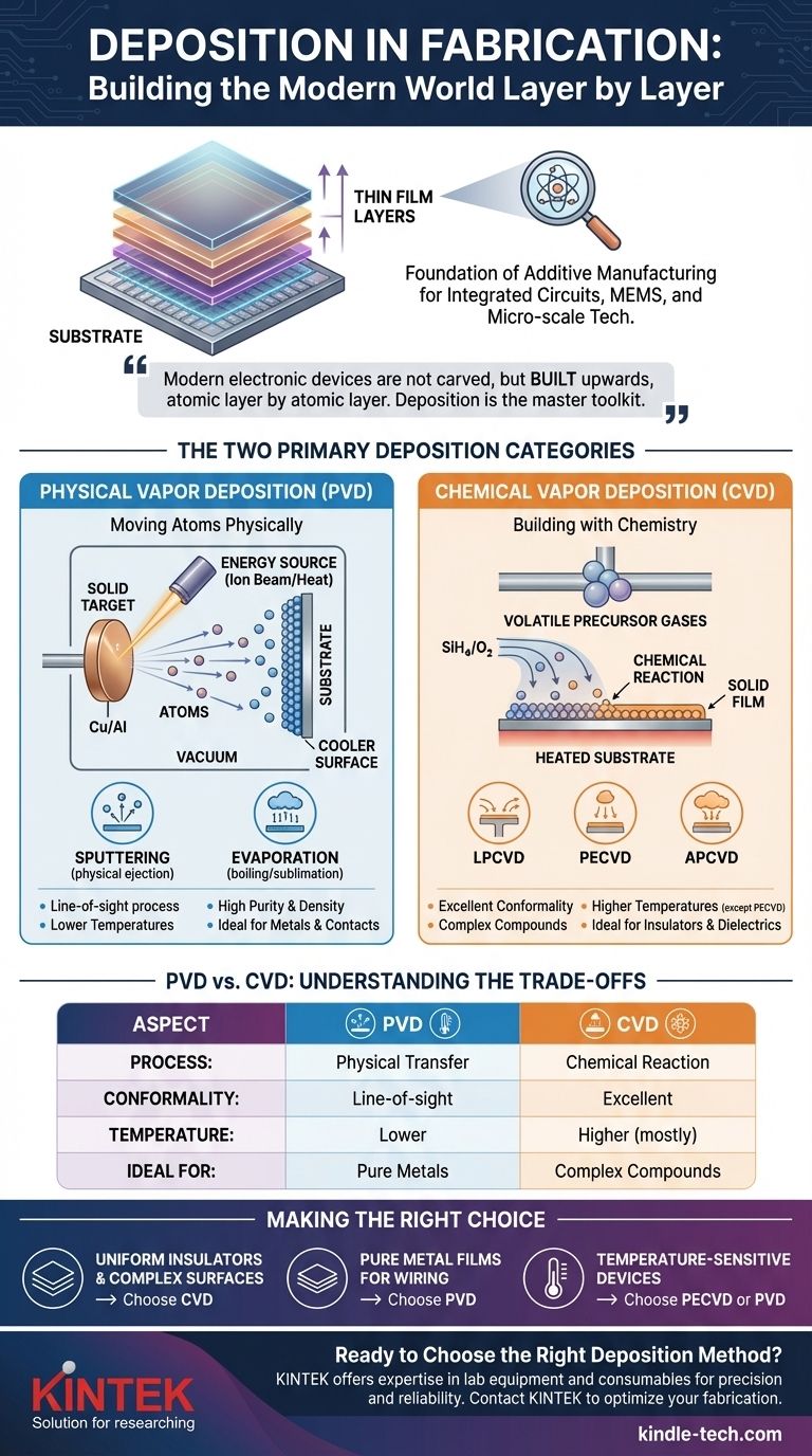
In the context of fabrication, deposition is the process of applying a thin film of material onto a substrate, such as a silicon wafer. It is a foundational "additive" manufacturing step used to build up the complex, layered structures that form integrated circuits, MEMS devices, and other micro-scale technologies.
The core concept to grasp is that modern electronic devices are not carved from a single block, but are built upwards, layer by atomic layer. Deposition is the master toolkit for adding these precise layers, and the specific technique chosen fundamentally determines the properties and performance of the final device.
The Role of Deposition: Building from the Ground Up
At its heart, fabrication is a cycle of adding material (deposition), patterning it (lithography), and removing material (etching). Deposition is the critical first step in this cycle, responsible for creating every functional layer of a device.
The Additive Principle
Think of deposition as a highly advanced form of 3D printing, but on an atomic scale. You start with a bare foundation—the substrate—and strategically add new layers of different materials, each with a specific electrical or structural purpose.
What Kinds of Layers?
These deposited films can be insulators (like silicon dioxide) to prevent electrical shorts, conductors (like copper or aluminum) to form wires and interconnects, or semiconductors (like polysilicon) to create transistors and other active components.
The Two Primary Deposition Categories
Nearly all deposition techniques fall into one of two major families, distinguished by how they get the material from a source to the substrate: Physical Vapor Deposition (PVD) and Chemical Vapor Deposition (CVD).
Physical Vapor Deposition (PVD): Moving Atoms Physically
In PVD, the material to be deposited starts as a solid target. This target is bombarded with energy, causing atoms to be physically knocked off or boiled off into a vapor. This vapor then travels through a vacuum and condenses as a thin film on the cooler substrate.
The two most common PVD methods are:
- Sputtering: An ion beam (like argon) bombards the target, physically ejecting atoms like microscopic billiard balls. This method creates dense, high-purity films.
- Evaporation: The source material is heated in a high vacuum until it evaporates (or sublimes), with the resulting vapor coating the substrate.
Chemical Vapor Deposition (CVD): Building with Chemistry
In CVD, the substrate is exposed to one or more volatile precursor gases. These gases react or decompose on the substrate's surface, leaving behind the desired solid material as a thin film.
Unlike PVD, the deposited material is the result of a chemical reaction. This allows for the creation of complex compound materials that would be difficult to sputter. CVD is known for producing highly uniform films that can conform perfectly to complex, three-dimensional surface features.
Understanding the Trade-offs: PVD vs. CVD
Engineers don't choose a deposition method randomly. The decision is a critical trade-off between the desired film properties, the underlying materials, and manufacturing cost.
Film Quality and Conformality
CVD processes generally produce films with excellent conformality. Because the precursor gases can reach every nook and cranny of a surface before reacting, the resulting film has a very uniform thickness, even over complex topography. PVD is a "line-of-sight" process and struggles to coat vertical sidewalls evenly.
Deposition Temperature
Traditional CVD often requires very high temperatures to drive the necessary chemical reactions. This heat can damage or alter previously deposited layers. PVD and specific types of CVD (like Plasma-Enhanced CVD or PECVD) can operate at much lower temperatures, making them suitable for later stages of fabrication.
Purity and Density
PVD, particularly sputtering, is excellent for depositing very pure and dense films, especially for metals. The physical bombardment process helps create a tightly packed film structure, which is ideal for creating robust electrical contacts.
Material Versatility
CVD offers greater flexibility in creating compound materials like silicon nitride or silicon dioxide, which are critical insulators in chip manufacturing. You simply change the recipe of precursor gases. PVD is typically limited to depositing materials that can be made into a solid target.
Making the Right Choice for Your Application
The choice between PVD and CVD hinges entirely on the specific goal for the layer being deposited.
- If your primary focus is creating a high-quality, uniform insulating layer over a complex surface: CVD is the definitive choice for its superior conformality.
- If your primary focus is depositing a pure metal film for wiring or electrical contacts: PVD, especially sputtering, is the industry standard for its high purity and film density.
- If your primary focus is coating a temperature-sensitive device or substrate: A low-temperature process like PECVD or PVD is required to avoid damaging the underlying structure.
Ultimately, deposition is the fundamental art of constructing the modern world, one precisely controlled atomic layer at a time.
Summary Table:
| Aspect | Physical Vapor Deposition (PVD) | Chemical Vapor Deposition (CVD) |
|---|---|---|
| Process | Physical transfer of atoms from a solid target | Chemical reaction of precursor gases on the substrate |
| Common Methods | Sputtering, Evaporation | LPCVD, PECVD, APCVD |
| Film Conformality | Line-of-sight; lower conformality | Excellent conformality over complex shapes |
| Typical Temperature | Lower temperatures | Higher temperatures (except PECVD) |
| Ideal For | Pure metal films, electrical contacts | Insulating layers, compound materials |
Ready to Choose the Right Deposition Method for Your Project?
At KINTEK, we understand that selecting the correct deposition technique is critical to the performance of your integrated circuits, MEMS devices, and other micro-scale technologies. Whether you require the high-purity metal films of PVD or the superior conformality of CVD for complex insulators, our expertise in lab equipment and consumables ensures you have the right tools for precision and reliability.
Let our specialists help you optimize your fabrication process. Contact KINTEK today to discuss your specific laboratory needs and discover how our solutions can enhance your research and production outcomes.
Visual Guide
Related Products
- RF PECVD System Radio Frequency Plasma-Enhanced Chemical Vapor Deposition RF PECVD
- Evaporation Boat for Organic Matter
- Thin-Layer Spectral Electrolysis Electrochemical Cell
- Side Window Optical Electrolytic Electrochemical Cell
- Reference Electrode Calomel Silver Chloride Mercury Sulfate for Laboratory Use
People Also Ask
- What is plasma CVD? Unlock Low-Temperature Thin Film Deposition for Sensitive Materials
- What is plasma chemical vapor deposition? A Low-Temperature Thin Film Coating Solution
- How does plasma enhance CVD? Unlock Low-Temperature, High-Quality Film Deposition
- What is the role of RF-PECVD in VFG preparation? Mastering Vertical Growth and Surface Functionality
- What is plasma enhanced chemical vapour deposition PECVD used for? Enable Low-Temp Thin Films for Electronics & Solar


