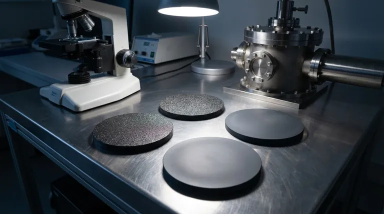
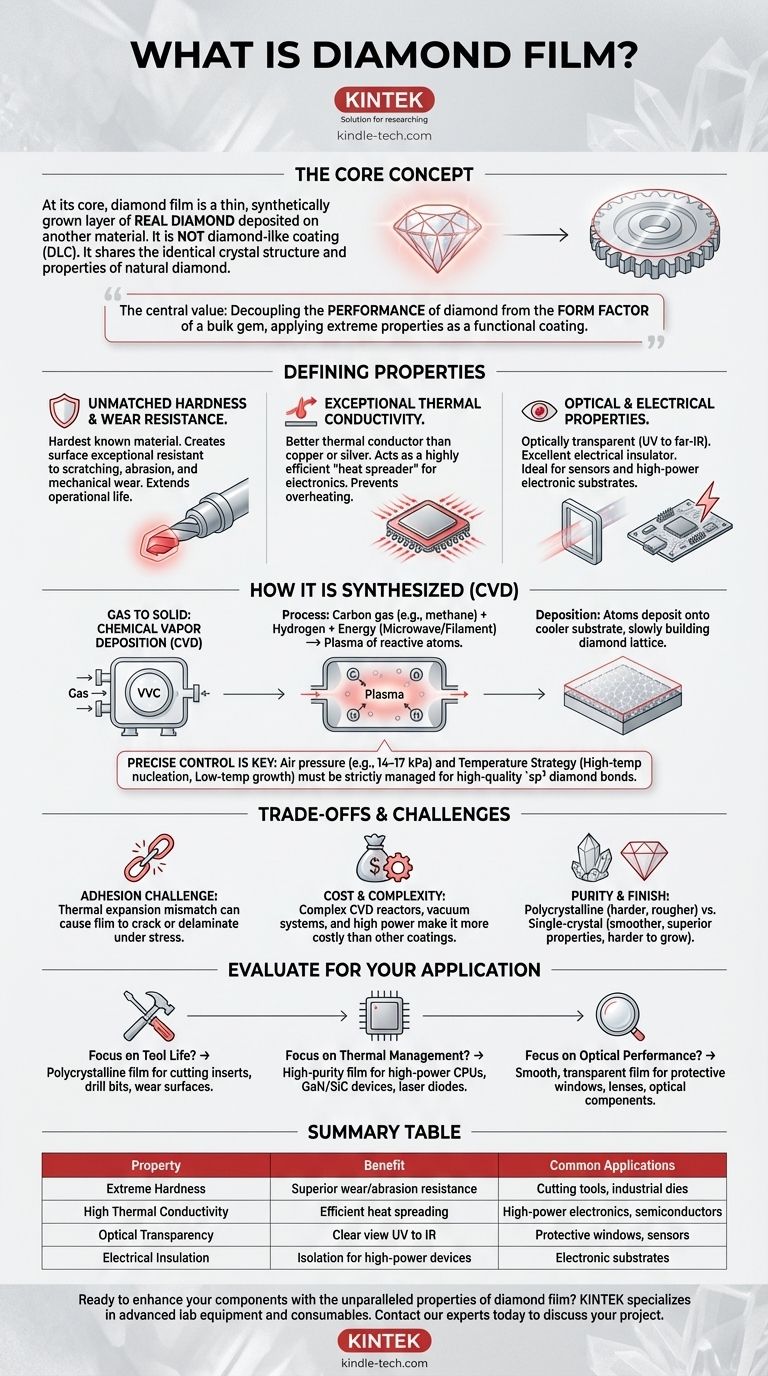
At its core, diamond film is a thin, synthetically grown layer of real diamond that is deposited onto the surface of another material. This is not a diamond-like coating (DLC), but a film with the identical crystal structure and properties of a natural diamond. The purpose is to impart diamond's extraordinary characteristics—such as extreme hardness and thermal conductivity—to materials that do not naturally possess them.
The central value of diamond film is its ability to decouple the performance of diamond from the form factor of a bulk gem. It allows engineers to apply the world's most extreme material as a functional coating, revolutionizing everything from electronics to industrial tools.
The Defining Properties of Diamond Film
To understand the value of diamond film, you must first understand the properties it brings to a substrate material. These are not merely incremental improvements; they are often order-of-magnitude enhancements.
Unmatched Hardness and Wear Resistance
Diamond is the hardest known material. When applied as a film, it creates a surface that is exceptionally resistant to scratching, abrasion, and mechanical wear.
This makes it an ideal coating for cutting tools, industrial dies, and any component subjected to intense friction. The film dramatically extends the operational life of the underlying part.
Exceptional Thermal Conductivity
Diamond is a better thermal conductor than any metal, including copper or silver. A thin layer of diamond film can act as a highly efficient "heat spreader."
This is critical in high-power electronics, where it can rapidly pull heat away from a sensitive semiconductor chip, preventing overheating and enabling higher performance and density.
Optical and Electrical Properties
Depending on its purity and structure, diamond film can be optically transparent across a wide spectrum of light, from ultraviolet to far-infrared.
Simultaneously, it is an excellent electrical insulator. This unique combination makes it valuable for protective windows on sensors in harsh environments or as a substrate for high-power, high-frequency electronic devices.
How Diamond Film Is Synthesized
Diamond film is not mined; it is grown in a lab using a process called Chemical Vapor Deposition (CVD). This process requires meticulously controlled conditions to force carbon atoms to arrange themselves into a diamond lattice instead of the more common graphite structure.
The Core Principle: Gas to Solid
In a typical CVD process, a substrate is placed in a vacuum chamber filled with a carbon-containing gas (like methane) and hydrogen.
Energy, usually from microwaves or a hot filament, is introduced to break down the gas molecules. This creates a plasma of reactive carbon and hydrogen atoms, which then deposit onto the cooler substrate surface, slowly building the diamond film atom by atom.
The Need for Precise Control
Growing high-quality diamond is a delicate balance. The process parameters must be managed within very narrow windows to ensure the carbon atoms form the strong sp³ bonds of diamond rather than the weak sp² bonds of graphite.
Controlling Pressure and Temperature
As an example of this precision, the chamber's air pressure must often be maintained in a specific range, such as 14–17 kPa. Even small deviations can compromise the film's quality.
Furthermore, a sophisticated temperature strategy, like high-temperature nucleation followed by low-temperature growth, is often used. The initial high heat helps the first diamond crystals form (nucleate) on the substrate, while a subsequent lower temperature promotes a steady, high-quality growth of the film.
Understanding the Trade-offs and Challenges
While its properties are exceptional, diamond film is not a universal solution. Its production and application come with significant technical challenges that create important trade-offs.
The Challenge of Adhesion
One of the biggest hurdles is getting the diamond film to stick firmly to the substrate. Many materials have a very different rate of thermal expansion than diamond.
As the component heats and cools during use, this mismatch in expansion can create immense stress at the interface, causing the film to crack or peel off (delaminate).
Cost and Complexity of Production
Diamond film CVD reactors are complex and expensive to build and operate. The process requires vacuum systems, precise gas handling, and high-power energy sources.
This makes diamond film significantly more costly than other hard coatings like titanium nitride or diamond-like carbon (DLC), limiting its use to applications where its superior performance justifies the expense.
Purity and Surface Finish
The performance of the film is directly tied to its quality. A polycrystalline film, made of many small, randomly oriented diamond crystals, is harder and cheaper to produce but can have a rough surface.
A single-crystal film is exceptionally smooth and has superior thermal and optical properties, but it is far more difficult and expensive to grow. Contamination with non-diamond carbon can also degrade performance.
How to Evaluate Diamond Film for Your Application
Choosing to use diamond film requires matching its specific benefits to a clear engineering goal. The type of film you need depends entirely on the problem you are trying to solve.
- If your primary focus is extending tool life: A hard, wear-resistant polycrystalline film on cutting inserts, drill bits, or wear surfaces is the most cost-effective choice.
- If your primary focus is thermal management in electronics: A high-purity, uniform film is essential for use as a heat spreader on high-power CPUs, GaN/SiC devices, or laser diodes.
- If your primary focus is optical performance in harsh environments: A smooth, low-scatter, optically transparent film is required for protective windows, lenses, or optical components.
Understanding these fundamentals allows you to leverage the unparalleled properties of diamond in a versatile and engineered form.
Summary Table:
| Property | Benefit | Common Applications |
|---|---|---|
| Extreme Hardness | Superior wear and abrasion resistance | Cutting tools, industrial dies |
| High Thermal Conductivity | Efficient heat spreading and dissipation | High-power electronics, semiconductors |
| Optical Transparency | Clear view from UV to IR spectrum | Protective windows, sensors |
| Electrical Insulation | Isolation for high-power devices | Electronic substrates |
Ready to enhance your components with the unparalleled properties of diamond film? KINTEK specializes in advanced lab equipment and consumables for materials science and coating technologies. Whether you're developing next-generation electronics, high-performance tools, or durable optical components, our expertise can help you integrate diamond film solutions effectively. Contact our experts today to discuss how we can support your project with precision and reliability.
Visual Guide
Related Products
- Custom CVD Diamond Coating for Lab Applications
- Laboratory CVD Boron Doped Diamond Materials
- CVD Diamond Optical Windows for Lab Applications
- CVD Diamond Wire Drawing Die Blanks for Precision Applications
- HFCVD Machine System Equipment for Drawing Die Nano-Diamond Coating
People Also Ask
- Can you coat something in diamond? Unlock Unmatched Hardness and Thermal Conductivity
- What are the types of CVD coating? A Guide to Choosing the Right Process
- What is CVD diamond coating? Grow a Super-Hard, High-Performance Diamond Layer
- What are the different CVD coating? A Guide to Thermal CVD, PECVD, and Specialized Methods
- How thick is CVD diamond coating? Balancing Durability and Stress for Optimal Performance


