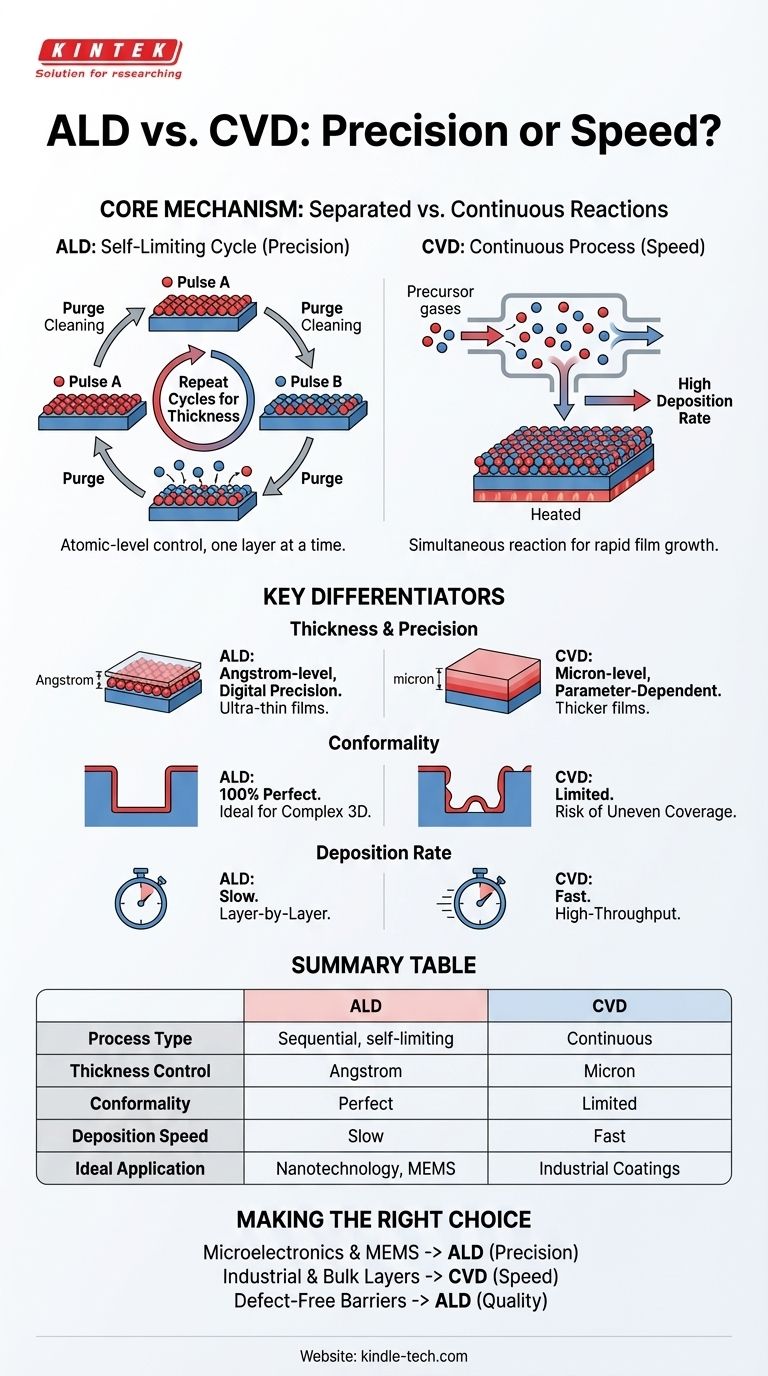
At their core, both Atomic Layer Deposition (ALD) and Chemical Vapor Deposition (CVD) are processes that build thin films from chemical reactions. The critical difference lies in how these reactions occur. CVD uses a continuous, simultaneous reaction of chemical precursors, while ALD separates these reactions into a precise, self-limiting, layer-by-layer sequence.
The choice between ALD and CVD is a fundamental trade-off between precision and speed. ALD offers unparalleled, atomic-level control over film thickness and uniformity, making it ideal for advanced applications. CVD offers high-speed deposition for thicker films where such extreme precision is unnecessary.
The Core Mechanism: Separated vs. Continuous Reactions
Understanding the process flow of each technique reveals why their capabilities are so different. Both belong to the broader category of chemical deposition, but their methodologies are fundamentally distinct.
How CVD Works: A Continuous Process
In a CVD process, one or more volatile chemical precursors are continuously fed into a reaction chamber.
These gases react simultaneously on and near the heated substrate surface, decomposing to form the desired solid film.
This continuous reaction allows for a very high deposition rate, making it efficient for growing thick films quickly.
How ALD Works: A Self-Limiting Cycle
ALD breaks the deposition down into a sequence of discrete, self-limiting steps. It is a cyclical process, with each cycle adding a single layer of atoms.
- Pulse A: The first precursor gas is introduced. It reacts with the substrate surface until every available reaction site is occupied, forming a single, uniform monolayer.
- Purge: Any remaining precursor gas and reaction byproducts are purged from the chamber.
- Pulse B: The second precursor gas is introduced. It reacts exclusively with the monolayer created in the first step.
- Purge: The chamber is purged again to remove excess gas and byproducts, completing one cycle.
This cycle is repeated hundreds or thousands of times to build a film of the desired thickness. Because each reaction only occurs on the available surface from the previous step, the process is self-limiting, ensuring atomic-level control.
Key Differentiators: Control vs. Speed
The mechanical differences between ALD and CVD lead to distinct advantages and disadvantages in film properties and process efficiency.
Film Thickness and Precision
ALD offers digital, angstrom-level control over thickness. The final film thickness is simply determined by the number of cycles performed, making it exceptionally precise and repeatable. It is the preferred method for ultra-thin films, often below 50 nanometers.
CVD thickness is controlled by process parameters like time, temperature, and gas flow rates. While suitable for films measured in microns, it lacks the fine, atomic-level precision of ALD.
Conformality and Uniformity
Conformality is the ability of a film to evenly coat complex, three-dimensional topographies.
ALD provides virtually perfect (100%) conformality. The self-limiting surface reactions allow the precursors to penetrate and coat the inside of extremely deep trenches or high-aspect-ratio structures with perfect uniformity.
CVD struggles with conformality. The continuous reaction means the openings of trenches are coated faster and thicker than the bottoms, which can lead to voids and inconsistent coverage on complex surfaces.
Deposition Rate and Throughput
CVD is significantly faster than ALD. Its continuous nature is optimized for high-volume production where thick films are needed and deposition speed directly impacts cost.
ALD is an inherently slow process due to the sequential pulse and purge steps. This makes it impractical and cost-prohibitive for depositing thick films but essential for applications where precision is non-negotiable.
Understanding the Trade-offs
Choosing a deposition technique requires an objective look at the limitations and practical considerations beyond just speed and control.
Material and Precursor Availability
CVD is a mature technology with decades of development behind it. This has resulted in a vast library of well-understood precursors for depositing a wide range of metals, dielectrics, and semiconductors.
ALD precursor chemistry is more complex. Finding two chemicals that react in the required self-limiting fashion can be challenging, so the range of available materials is more limited, though it is an active and expanding area of research.
Film Quality and Density
ALD films are typically of superior quality. The slow, layer-by-layer growth and often lower process temperatures result in films that are highly dense, pinhole-free, and exceptionally pure.
CVD films can be of high quality, but their properties are more sensitive to process conditions. The higher deposition rates can sometimes lead to lower film density or the incorporation of impurities.
Making the Right Choice for Your Application
The decision between ALD and CVD is driven entirely by your project's primary technical requirement.
- If your primary focus is cutting-edge microelectronics, MEMS, or nanotechnology: Choose ALD for its unparalleled thickness control and ability to uniformly coat high-aspect-ratio features.
- If your primary focus is industrial protective coatings or bulk semiconductor layers: Choose CVD for its high deposition rate and cost-effectiveness in producing thicker films.
- If your primary focus is a defect-free, highly dense barrier layer on a sensitive substrate: Lean towards ALD, as its precise, low-temperature process produces films of superior quality and purity.
Ultimately, understanding this fundamental opposition—ALD's atomic precision versus CVD's industrial speed—is the key to selecting the correct deposition strategy.
Summary Table:
| Feature | Atomic Layer Deposition (ALD) | Chemical Vapor Deposition (CVD) |
|---|---|---|
| Process Type | Sequential, self-limiting cycle | Continuous, simultaneous reaction |
| Thickness Control | Angstrom-level, digital precision | Micron-level, parameter-dependent |
| Conformality | Perfect (100%), ideal for complex 3D structures | Limited, can lead to uneven coverage |
| Deposition Speed | Slow, layer-by-layer | Fast, high-throughput |
| Ideal Application | Ultra-thin films, nanotechnology, MEMS | Thick coatings, industrial applications |
Struggling to choose the right deposition technique for your lab's specific needs? KINTEK specializes in providing precision lab equipment and consumables for both ALD and CVD processes. Our experts can help you select the ideal solution to achieve superior film quality, whether you require atomic-level control or high-speed deposition. Contact our team today to discuss how we can enhance your laboratory's capabilities and efficiency.
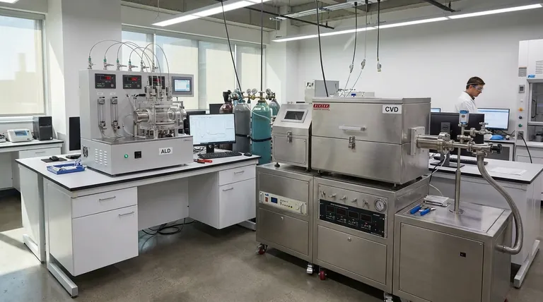
Visual Guide