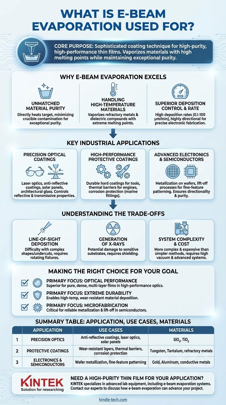
At its core, electron beam (e-beam) evaporation is a sophisticated coating technique used to deposit high-purity, high-performance thin films onto surfaces. Its primary applications range from creating precision optical coatings for laser optics and eyeglasses to applying durable, wear-resistant layers on components for the aerospace, automotive, and manufacturing industries.
The central reason to choose e-beam evaporation is for its unique ability to vaporize materials with very high melting points while maintaining exceptional purity. This makes it the ideal process for creating advanced films that are difficult, if not impossible, to achieve with simpler thermal techniques.
Why E-Beam Evaporation Excels
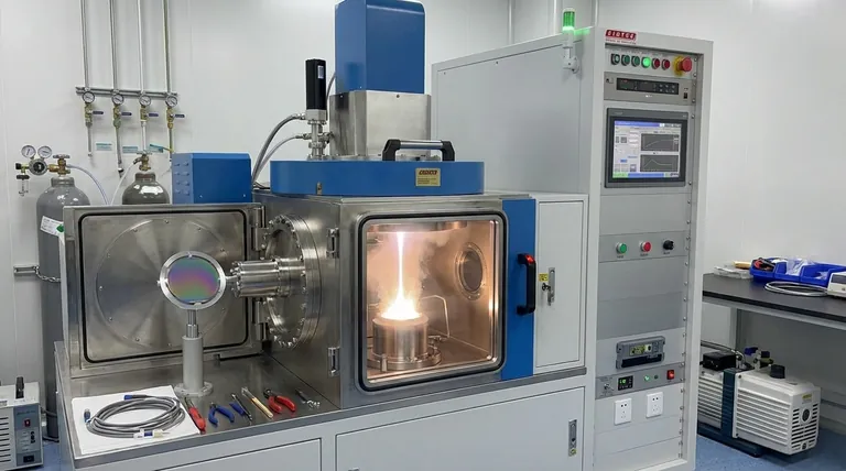
To understand its applications, we must first understand its fundamental advantage. E-beam evaporation uses a high-energy beam of electrons, magnetically guided in a vacuum, to heat and vaporize a source material. This focused heating mechanism is the source of its key strengths.
Unmatched Material Purity
The electron beam directly heats only the target material in its crucible. This minimizes contact with the crucible walls, drastically reducing the risk of contamination and resulting in exceptionally high-purity thin films.
Handling High-Temperature Materials
The intense, localized energy of the electron beam can melt and vaporize materials with extremely high melting points, such as refractory metals (like tungsten and tantalum) and dielectric compounds (like silicon dioxide and titanium dioxide).
Superior Deposition Control and Rate
E-beam systems allow for very high deposition rates, ranging from 0.1 to 100 micrometers per minute, enabling efficient high-volume production. The process is also highly directional, which is a critical advantage for certain electronic fabrication techniques like lift-off patterning.
Key Industrial Applications
The unique capabilities of e-beam evaporation make it indispensable across several high-tech sectors for tailoring the surface properties of components.
Precision Optical Coatings
This is a primary use case. By depositing precise, multi-layered films of materials like metal oxides, e-beam evaporation is used to control the reflective and transmissive properties of surfaces.
This is critical for manufacturing laser optics, anti-reflective coatings on eyeglasses, solar panels, and specialized architectural glass.
High-Performance Protective Coatings
In demanding industries like aerospace and automotive, components require protection from extreme conditions. E-beam evaporation is used to apply durable hard coatings to cutting tools and thermal barrier coatings to engine parts.
It also creates chemical barriers for components exposed to corrosive environments, such as marine fittings.
Advanced Electronics and Semiconductors
The directionality and purity of the e-beam process are essential in electronics manufacturing. It is a standard method for metallization, where conductive layers are deposited onto wafers.
Its line-of-sight deposition is also ideal for lift-off processes, a method for patterning films with very fine features.
Understanding the Trade-offs
While powerful, e-beam evaporation is not a universal solution. An objective assessment requires understanding its limitations.
Line-of-Sight Deposition
The vaporized material travels in a straight line from the source to the substrate. This means it cannot easily coat complex, three-dimensional shapes with undercuts, which can result in "shadowing" and non-uniform coverage without complex rotating fixtures (planetaries).
Generation of X-rays
The impact of high-energy electrons on the source material generates X-rays. This can potentially damage sensitive substrates or electronic components and requires appropriate shielding for safe operation.
System Complexity and Cost
E-beam evaporation systems are more complex and expensive than simpler deposition methods like resistive thermal evaporation. The process requires a high-vacuum environment and sophisticated power and magnetic control systems.
Making the Right Choice for Your Goal
The decision to use e-beam evaporation hinges on your specific material and performance requirements.
- If your primary focus is optical performance: E-beam is the superior choice for creating the pure, dense, and precisely controlled multi-layer films required for high-performance optics.
- If your primary focus is extreme durability: E-beam enables the deposition of high-temperature, wear-resistant materials that cannot be processed with other thermal methods.
- If your primary focus is microfabrication: The high purity and directionality of e-beam evaporation are critical for reliable metallization and lift-off processes in semiconductor manufacturing.
Ultimately, e-beam evaporation provides a level of precision and material versatility essential for engineering the surfaces of today's most advanced components.
Summary Table:
| Application Area | Key Use Cases | Key Materials Deposited |
|---|---|---|
| Precision Optics | Anti-reflective coatings, laser optics, solar panels | Silicon Dioxide (SiO₂), Titanium Dioxide (TiO₂) |
| Protective Coatings | Wear-resistant layers, thermal barriers, corrosion protection | Tungsten, Tantalum, other refractory metals |
| Electronics & Semiconductors | Wafer metallization, fine-feature patterning (lift-off) | Gold, Aluminum, other conductive metals |
Need a high-purity thin film for your demanding application?
KINTEK specializes in advanced lab equipment, including e-beam evaporation systems, to meet the precise needs of research and production laboratories. Whether you are developing next-generation optics, durable aerospace components, or sophisticated semiconductor devices, our expertise ensures you achieve the material performance you require.
Contact our experts today to discuss how e-beam evaporation can advance your project.
Visual Guide
Related Products
- Electron Beam Evaporation Coating Oxygen-Free Copper Crucible and Evaporation Boat
- Electron Beam Evaporation Coating Tungsten Crucible and Molybdenum Crucible for High Temperature Applications
- Electron Beam Evaporation Coating Gold Plating Tungsten Molybdenum Crucible for Evaporation
- Electron Beam Evaporation Coating Conductive Boron Nitride Crucible BN Crucible
- E Beam Crucibles Electron Gun Beam Crucible for Evaporation
People Also Ask
- What are the applications of electron beams? From Nanoscale Imaging to Industrial Manufacturing
- What is the current of e-beam evaporation? A Guide to High-Purity Thin Film Deposition
- What is the temperature of e-beam evaporation? Mastering the Two-Zone Thermal Process for Precision Films
- What is the voltage of e-beam evaporation? Achieve Precise Thin-Film Deposition
- How is an electron beam evaporator cooled during deposition? Essential Thermal Management for Stable Processes


