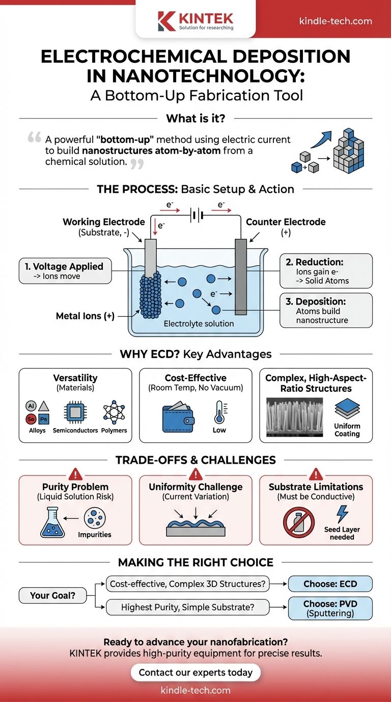
In nanotechnology, electrochemical deposition is a powerful "bottom-up" fabrication method that uses a controlled electric current to build nanostructures atom-by-atom from a chemical solution. Unlike techniques that carve material away, this process precisely assembles materials like nanowires, thin films, and nanotubes directly onto a conductive surface.
At its core, electrochemical deposition is a versatile and low-cost tool for growing complex nanostructures. It offers remarkable control over shape and composition but requires careful management of solution chemistry and electrical parameters to achieve high purity and uniformity.
The Fundamental Principle of Electrochemical Deposition
Electrochemical deposition (ECD), also known as electroplating or electrodeposition, translates electrical energy into chemical change, effectively "growing" a solid material from a liquid precursor. It's a foundational process in materials science, adapted with high precision for the nanoscale.
The Basic Setup
The process operates with a few key components in a solution called an electrolyte. This solution contains dissolved metal salts, which provide the positively charged ions (cations) that will form the final structure.
Immersed in this electrolyte are at least two electrodes: the working electrode (the substrate you want to coat) and the counter electrode, which completes the electrical circuit.
The Process in Action
When a voltage is applied, the positively charged metal ions in the electrolyte are drawn to the negatively charged working electrode. At the surface of this substrate, the ions gain electrons in a chemical reaction known as reduction.
This reduction transforms the dissolved ions into solid, neutral metal atoms. These atoms then deposit onto the substrate surface, building up the desired film or nanostructure one atomic layer at a time.
From Atoms to Nanostructures
The power of ECD in nanotechnology comes from the precise control it offers. By carefully tuning the applied voltage, current density, electrolyte composition, and deposition time, researchers can dictate the final structure's properties.
This allows for the creation of highly ordered structures, such as vertically aligned nanowires, porous nanofoams, or ultra-thin films with specific grain sizes, all by managing the electrical and chemical environment.
Why ECD is a Key Tool in Nanotechnology
While other methods like magnetron sputtering exist, ECD holds a unique place in the nanotechnologist's toolkit due to its distinct advantages in specific applications.
Unmatched Versatility
ECD is not limited to simple metals. The technique can be used to deposit a vast range of materials, including metal alloys, semiconductors, conductive polymers, and composite materials, simply by changing the composition of the electrolyte solution.
Cost-Effectiveness and Simplicity
A major advantage of ECD is that it operates at or near room temperature and atmospheric pressure. It does not require expensive high-vacuum chambers or high-temperature equipment, making it a significantly more accessible and cost-effective method for both research and industrial-scale production.
Building Complex, High-Aspect-Ratio Structures
ECD excels at creating complex three-dimensional and high-aspect-ratio nanostructures. It can uniformly coat intricate shapes and grow structures like dense arrays of nanowires, which are extremely difficult to produce with line-of-sight methods like sputtering.
Understanding the Trade-offs and Challenges
No single technique is perfect for every application. To use ECD effectively, it's critical to understand its limitations, especially when compared to physical vapor deposition (PVD) methods like sputtering.
The Purity Problem
Because deposition occurs in a liquid solution, there is a higher risk of incorporating impurities from the electrolyte into the growing nanostructure. Achieving the ultra-high purity possible with vacuum-based PVD methods requires extremely clean chemicals and careful process control.
The Challenge of Uniformity
Achieving a perfectly uniform coating thickness across a large or complex-shaped substrate can be difficult. Electrical current density can vary at edges and in corners, leading to non-uniform growth if the process is not carefully engineered.
Substrate Limitations
The most basic form of ECD requires the substrate to be electrically conductive. While insulating materials can be coated by first applying a thin conductive seed layer, this adds a step to the process.
Making the Right Choice for Your Goal
Selecting the correct fabrication method depends entirely on your project's specific priorities.
- If your primary focus is cost-effective production of complex 3D nanostructures: Electrochemical deposition is often the superior choice due to its low equipment cost and ability to coat non-flat surfaces.
- If your primary focus is achieving the highest possible material purity on a simple substrate: A physical vapor deposition method like magnetron sputtering is likely the better option.
- If your primary focus is creating large arrays of nanowires or nanotubes: Electrochemical deposition provides one of the most direct and scalable methods available.
Understanding these fundamental principles allows you to select the right tool for the job, moving your project forward with confidence and precision.
Summary Table:
| Aspect | Description |
|---|---|
| Process | A 'bottom-up' method using electric current to deposit material from a solution. |
| Key Materials | Metals, alloys, semiconductors, conductive polymers, composites. |
| Primary Advantages | Cost-effective, versatile, excellent for 3D/high-aspect-ratio structures. |
| Key Considerations | Requires conductive substrate; purity and uniformity need careful control. |
Ready to advance your nanofabrication research?
Electrochemical deposition is a powerful tool for creating complex nanostructures like nanowires and thin films. At KINTEK, we specialize in providing the high-purity lab equipment and consumables you need to master this technique and achieve precise, reliable results.
Contact our experts today to discuss how our solutions can support your specific laboratory goals and streamline your R&D process.
Visual Guide
Related Products
- RF PECVD System Radio Frequency Plasma-Enhanced Chemical Vapor Deposition RF PECVD
- HFCVD Machine System Equipment for Drawing Die Nano-Diamond Coating
- Chemical Vapor Deposition CVD Equipment System Chamber Slide PECVD Tube Furnace with Liquid Gasifier PECVD Machine
- Customer Made Versatile CVD Tube Furnace Chemical Vapor Deposition Chamber System Equipment
- Inclined Rotary Plasma Enhanced Chemical Vapor Deposition PECVD Equipment Tube Furnace Machine
People Also Ask
- What is plasma CVD? Unlock Low-Temperature Thin Film Deposition for Sensitive Materials
- What is plasma enhanced chemical vapour deposition PECVD used for? Enable Low-Temp Thin Films for Electronics & Solar
- What is plasma enhanced chemical Vapour deposition process used for fabrication of? A Guide to Low-Temperature Thin Films
- Why is a Matching Network Indispensable in RF-PECVD for Siloxane Films? Ensure Stable Plasma and Uniform Deposition
- What is an example of PECVD? RF-PECVD for High-Quality Thin Film Deposition