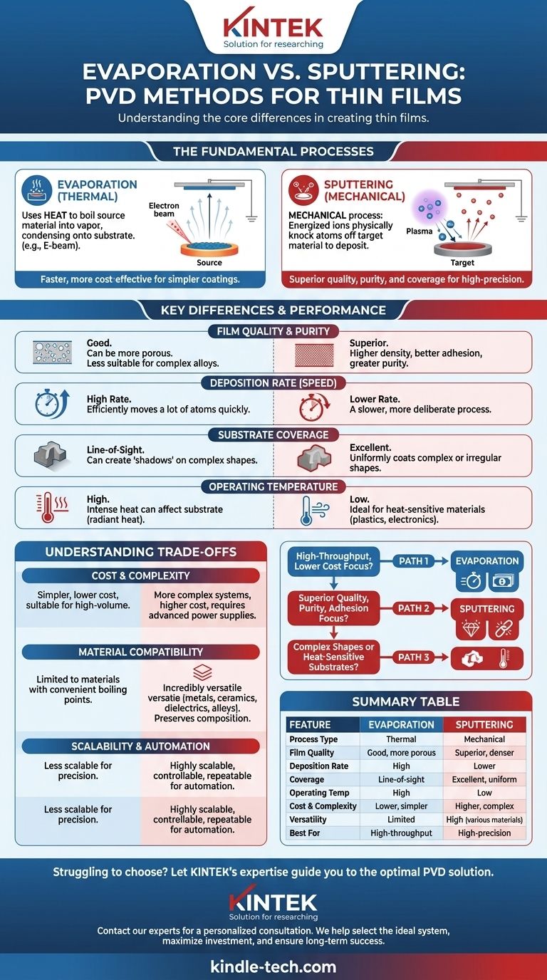
At their core, evaporation and sputtering are two distinct methods of physical vapor deposition (PVD) used to create thin films. Evaporation uses heat—often from an electron beam—to boil a source material into a vapor, which then condenses onto a substrate. Sputtering, in contrast, is a mechanical process where energized ions are used to physically knock atoms off a target material, which then travel and deposit onto the substrate.
The fundamental choice between these methods comes down to a trade-off. Evaporation is typically faster and more cost-effective for simpler coatings, while sputtering provides superior film quality, purity, and coverage, making it ideal for high-precision applications.
How Each Process Works: A Fundamental Comparison
Both techniques create a thin film atom-by-atom, but their methods of liberating those atoms from the source material are fundamentally different.
Evaporation: Heating to Vaporize
Evaporation is an entirely thermal process. A source material is placed inside a high-vacuum chamber and heated until it literally boils and turns into a gas.
This vapor then travels in a straight line until it makes contact with the cooler substrate, where it condenses back into a solid, forming a thin, uniform layer. The most common method for this is e-beam evaporation, which uses a focused beam of electrons to heat the material.
Sputtering: A Billiard Ball Analogy
Sputtering is a physical or mechanical process driven by momentum transfer. Think of it like a microscopic game of pool.
Inside a vacuum chamber, a high-energy plasma is created (typically with an inert gas like argon). These energized gas ions are accelerated and smashed into a target made of the desired coating material.
This collision physically knocks atoms loose from the target, "sputtering" them away. These ejected atoms then travel and deposit onto the substrate, building the thin film.
Key Differences in Performance and Outcome
The differences in how atoms are liberated lead to significant variations in the final film's characteristics and the process's efficiency.
Film Quality and Purity
Sputtering generally produces films with higher density, better adhesion, and greater purity. The energetic nature of the sputtered atoms helps them form a more tightly packed structure on the substrate.
Evaporation can sometimes result in more porous films, and since it relies on melting and boiling, it is less suitable for precisely depositing complex compounds or alloys without altering their composition.
Deposition Rate (Speed)
Evaporation almost always has a much higher deposition rate. Boiling a material to create a dense vapor is a very efficient way to move a lot of atoms quickly.
Sputtering is a slower, more deliberate process of knocking atoms off one by one, resulting in a lower deposition rate.
Substrate Coverage
Sputtering provides significantly better coating coverage, especially on substrates with complex or irregular shapes. Because sputtered atoms are ejected in various directions, they can coat surfaces that are not in a direct "line of sight" from the source.
Evaporation is highly directional. The vapor travels in a straight line, which can create "shadows" on complex parts, leading to an uneven coating.
Operating Temperature
Sputtering is a much lower-temperature process. The substrate does not need to be heated significantly, which makes it ideal for coating heat-sensitive materials like plastics or electronics.
Evaporation involves intense heat to vaporize the source material, which can radiate and heat the substrate, limiting its use with certain materials.
Understanding the Trade-offs
Choosing a method requires balancing your technical requirements with practical constraints like budget and production volume.
Cost and System Complexity
Evaporation systems are often simpler and more cost-effective, particularly for high-volume production where speed is a primary driver of cost.
Sputtering equipment can be more complex due to the need for high-voltage power supplies, magnetic fields to confine plasma, and more sophisticated vacuum systems.
Material Compatibility
Sputtering is incredibly versatile and can be used to deposit a vast range of materials, including metals, ceramics, dielectrics, and complex alloys. Since it doesn't melt the target, the material's original composition is preserved in the final film.
Evaporation is more limited. It works best with materials that have a convenient boiling point and won't decompose or react when heated to a gaseous state.
Scalability and Automation
Sputtering is considered more scalable and better suited for automated, industrial applications. The process is highly controllable and repeatable, which is critical for high-precision manufacturing.
Making the Right Choice for Your Application
Your final decision should be guided by the single most important outcome you need to achieve.
- If your primary focus is high-throughput production and lower cost: Evaporation is often the most practical and economical choice.
- If your primary focus is superior film quality, purity, and adhesion: Sputtering is the definitive technical solution for demanding applications.
- If you are coating complex shapes or heat-sensitive substrates: Sputtering's excellent coverage and low-temperature operation give it a clear advantage.
Ultimately, understanding the distinct physical mechanisms of each process empowers you to select the tool that best aligns with your project's specific goals.
Summary Table:
| Feature | Evaporation | Sputtering |
|---|---|---|
| Process Type | Thermal (heating to vaporize) | Mechanical (momentum transfer) |
| Film Quality | Good; can be more porous | Superior; denser, better adhesion |
| Deposition Rate | High | Lower |
| Substrate Coverage | Line-of-sight; shadows on complex shapes | Excellent; coats complex shapes uniformly |
| Operating Temperature | High (can heat substrate) | Low (ideal for heat-sensitive materials) |
| Cost & Complexity | Generally lower cost, simpler systems | Higher cost, more complex equipment |
| Material Versatility | Limited; best for simple materials | High; metals, ceramics, alloys, dielectrics |
| Best For | High-throughput, cost-effective coatings | High-precision, high-quality films |
Struggling to choose between evaporation and sputtering for your thin film application? Let KINTEK's expertise guide you to the optimal solution.
As your dedicated partner in lab equipment and consumables, we understand that the right PVD method is critical to your project's success—whether you prioritize speed, cost, or unparalleled film quality. Our team provides not just industry-leading equipment, but also the technical support to ensure you achieve precise, reliable results.
We help you:
- Select the ideal system based on your specific material, substrate, and performance requirements.
- Maximize your investment with solutions tailored for research, development, or high-volume production.
- Ensure long-term success with ongoing support, maintenance, and consumables for your laboratory needs.
Don't leave your coating results to chance. Contact our experts today for a personalized consultation and discover how KINTEK can enhance your laboratory's capabilities.
Visual Guide