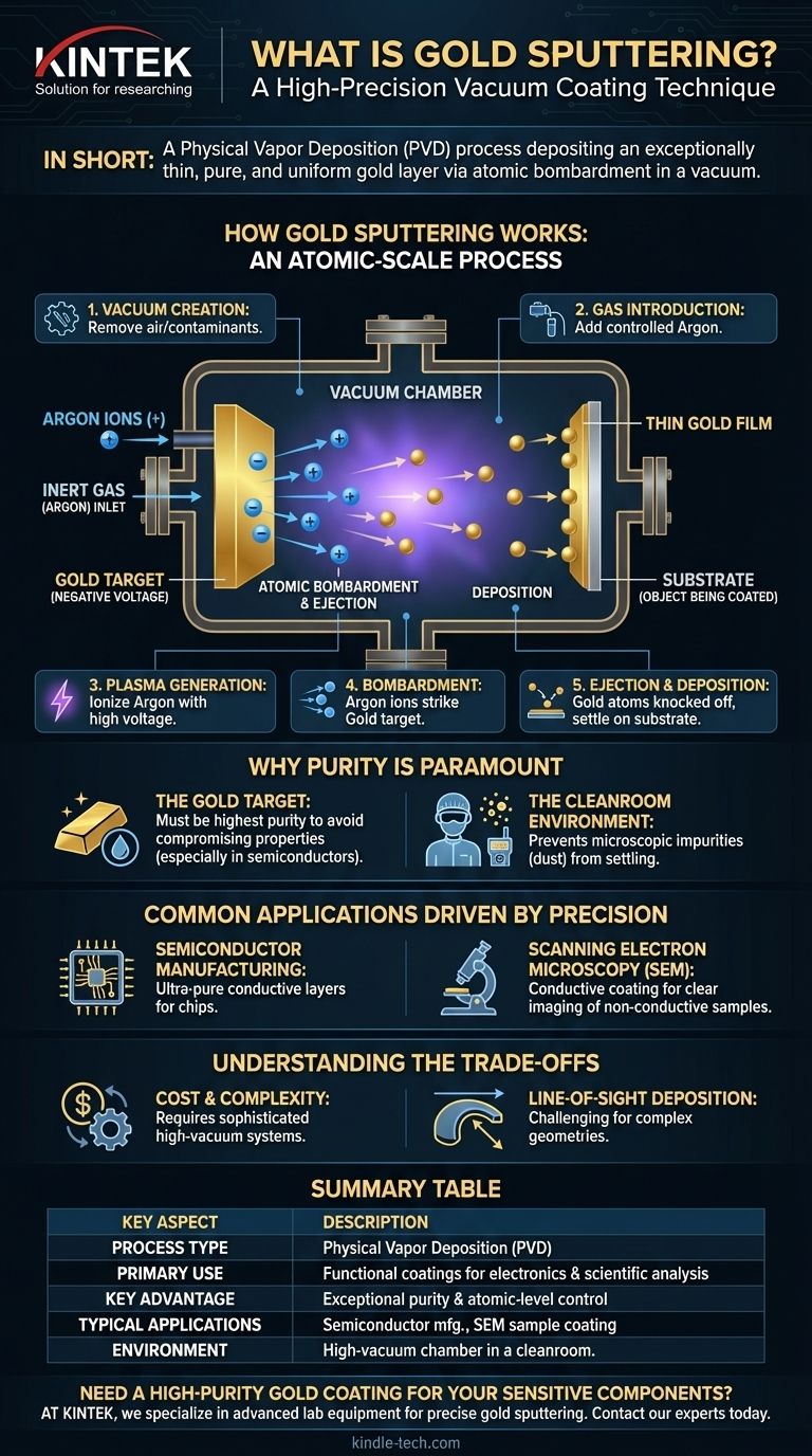
In short, gold sputtering is a high-precision vacuum coating technique. It is a physical process used to deposit an exceptionally thin, pure, and uniform layer of gold onto a surface. This is not a chemical plating or dipping process; instead, it works by physically knocking individual gold atoms from a source and transferring them onto the target object.
The core principle of gold sputtering is using energized gas ions to bombard a solid gold target in a vacuum. This impact ejects gold atoms, which then travel and settle onto a substrate, forming an atomic-level thin film with unmatched purity and control.
How Gold Sputtering Works: An Atomic-Scale Process
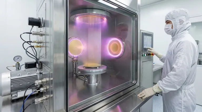
The entire process occurs inside a sealed vacuum chamber to prevent contamination and ensure the gold atoms can travel without obstruction. It is a form of Physical Vapor Deposition (PVD).
Step 1: Creating the Vacuum
The first step is to evacuate the chamber, removing almost every air molecule. This is critical because any residual particles, like oxygen or even dust, could react with the gold or contaminate the final film.
Step 2: Introducing an Inert Gas
Once a vacuum is established, a small, controlled amount of an inert process gas is introduced. Argon is most commonly used because it is heavy and does not chemically react with other materials.
Step 3: Generating a Plasma
A strong negative electrical voltage is applied to the solid block of source material, known as the gold target. This high voltage ionizes the argon gas atoms, stripping them of an electron and giving them a positive charge, which creates a controlled plasma.
Step 4: Atomic Bombardment
The positively charged argon ions are now powerfully attracted to the negatively charged gold target. They accelerate across the chamber and collide with the gold target with significant force.
Step 5: Ejection and Deposition
This bombardment is a physical transfer of energy. The impact has enough force to knock, or "sputter," individual gold atoms off the target. These ejected gold atoms then travel through the vacuum and land on the substrate (the object being coated), gradually building up a thin, uniform film.
Why Purity is a Non-Negotiable Requirement
The quality of a sputtered film is directly tied to the purity of the materials and the environment. For high-technology applications, this is the most critical factor.
The Gold Target
The gold source material must be of the highest possible purity. Even trace impurities within the target can be sputtered along with the gold, compromising the electrical or thermal properties of the final coating. This is especially vital in semiconductor production.
The Cleanroom Environment
Gold sputtering is performed in a clean room to prevent microscopic impurities from settling on the substrate. A single speck of dust can render a sensitive electronic component useless or skew results in scientific analysis, such as scanning electron microscopy.
Common Applications Driven by Precision
Gold sputtering is not used for decorative items; it is a functional process reserved for applications where performance and precision are paramount.
Semiconductor Manufacturing
Gold is an excellent electrical and thermal conductor. Sputtering is used to apply ultra-pure, single-atom-thick conductive layers on circuit chips, boards, and other sensitive electronic components.
Scanning Electron Microscopy (SEM)
To get a clear image of a non-conductive sample (like a biological specimen or ceramic) in an SEM, it must first be coated with a conductive material. Gold sputtering applies a very thin layer that allows electrical charge to dissipate, resulting in sharp, detailed images.
Understanding the Trade-offs
While highly effective, gold sputtering has specific characteristics that make it suitable for some tasks but not others.
Cost and Complexity
Sputtering systems are sophisticated pieces of equipment that require a high vacuum, precise gas control, and a clean environment. This makes the process and machinery significantly more expensive than simpler coating methods like electroplating.
Line-of-Sight Deposition
The sputtered atoms travel in a relatively straight line from the target to the substrate. This means it can be challenging to achieve a perfectly uniform coating on objects with complex geometries, such as deep holes or sharp interior corners.
Making the Right Choice for Your Goal
Deciding whether to use gold sputtering depends entirely on the technical requirements of the final product.
- If your primary focus is ultimate purity and conductivity: Gold sputtering is the superior choice for advanced semiconductors and sensitive electronics where performance cannot be compromised.
- If your primary focus is preparing a non-conductive sample for microscopy: Sputtering is the standard industry practice for creating the thin, uniform conductive layer required for high-quality SEM imaging.
- If your primary focus is a simple, cost-effective metallic coating: A different process like electroplating is likely more suitable, as sputtering is a high-precision technique reserved for demanding applications.
Ultimately, gold sputtering is the definitive method when precision, purity, and atomic-level control over a gold coating are paramount.
Summary Table:
| Key Aspect | Description |
|---|---|
| Process Type | Physical Vapor Deposition (PVD) |
| Primary Use | Functional coatings for electronics & scientific analysis |
| Key Advantage | Exceptional purity and atomic-level control |
| Typical Applications | Semiconductor manufacturing, SEM sample coating |
| Environment | High-vacuum chamber in a cleanroom |
Need a high-purity gold coating for your sensitive electronic components or SEM samples?
At KINTEK, we specialize in providing the advanced lab equipment and consumables required for precise gold sputtering processes. Our expertise ensures you achieve the unmatched purity and conductivity your applications demand.
Contact our experts today to discuss how our solutions can enhance your laboratory's capabilities and deliver reliable, high-performance results.
Visual Guide
Related Products
- Electron Beam Evaporation Coating Gold Plating Tungsten Molybdenum Crucible for Evaporation
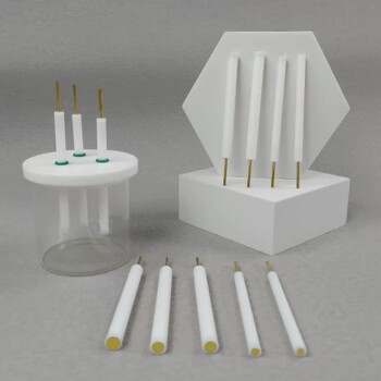
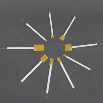
- Gold Disc Electrode
- Gold Electrochemical Sheet Electrode Gold Electrode
People Also Ask
- What is the process of e-beam coating? Achieve High-Purity, Precise Thin Films for Your Lab
- What is the temperature of e-beam evaporation? Mastering the Two-Zone Thermal Process for Precision Films
- What materials are used in electron beam evaporation? Master High-Purity Thin Film Deposition
- What is e-beam evaporation? Achieve High-Purity Thin Film Deposition for Your Lab
- What is the container that holds the metal source material called in e-beam evaporation? Ensure Purity and Quality in Your Thin-Film Deposition