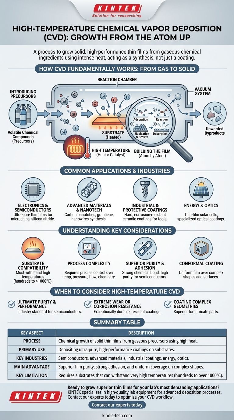
At its core, high-temperature chemical vapor deposition (CVD) is a process used to grow a solid, high-performance thin film onto a surface from chemical ingredients in a gaseous state. A substrate, or the part to be coated, is heated to a high temperature inside a reaction chamber and exposed to volatile precursor gases. The intense heat acts as the catalyst, causing a chemical reaction that deposits a new, solid material directly onto the substrate's surface, atom by atom.
The critical concept to understand is that CVD is not simply a coating process like painting; it is a synthesis process. You are chemically growing a new, engineered layer with superior purity and adhesion directly onto an object's surface using heat to drive the transformation from gas to solid.
How CVD Fundamentally Works: From Gas to Solid
The CVD process might seem complex, but it can be broken down into a series of logical, controlled steps. It all happens within a highly controlled environment to ensure the purity and quality of the final film.
The Controlled Environment
The entire process takes place within a sealed reaction chamber, which is typically held under a vacuum. This vacuum environment removes contaminants and allows for precise control over the gases and pressures involved.
Introducing the Precursors
Volatile chemical compounds, known as precursors, are injected into the chamber in gaseous form. These gases contain the specific atoms (like silicon, carbon, or titanium) that will eventually form the solid film.
The Role of High Temperature
The substrate is heated to a specific, often very high, temperature. This heat provides the necessary energy for thermal decomposition, breaking down the precursor gases and initiating the desired chemical reactions right at the substrate's surface.
Building the Film, Atom by Atom
Once the precursor gases react, a highly structured sequence occurs at the molecular level:
- Adsorption: The reactive gas molecules stick to the hot substrate surface.
- Reaction: Surface-catalyzed reactions create the desired solid material and gaseous byproducts.
- Nucleation & Growth: The solid atoms diffuse across the surface to form stable clusters (nuclei), which then grow into a continuous, thin film.
- Desorption: Unwanted gaseous byproducts are released from the surface and transported away by the vacuum system.
Common Applications and Industries
Because CVD can produce extremely pure, dense, and durable films, it has become a foundational technology in numerous high-tech fields.
Electronics and Semiconductors
This is one of the most common uses for CVD. It is essential for depositing the ultra-pure thin films of silicon, silicon nitride, and other materials that form the basis of microchips and integrated circuits.
Advanced Materials and Nanotechnology
CVD is a leading method for growing highly structured materials with unique properties. This includes the synthesis of carbon nanotubes, graphene, and various nanowires for next-generation electronics and composites.
Industrial and Protective Coatings
The process is used to apply exceptionally hard and corrosion-resistant ceramic coatings, like titanium nitride, onto cutting tools and industrial components. This dramatically increases their lifespan and performance.
Energy and Optics
In the energy sector, CVD is used to deposit the critical photovoltaic materials that make up thin-film solar cells. It is also used to apply specialized coatings to glass and other optical components.
Understanding the Key Considerations
While powerful, CVD is a highly technical process with specific requirements and trade-offs that determine its suitability for a given application.
Substrate Compatibility
The "high-temperature" aspect is a critical limitation. The base material, or substrate, must be able to withstand the required reaction temperature (which can be several hundred to over a thousand degrees Celsius) without melting, warping, or degrading.
Process Complexity
Achieving a high-quality, uniform film requires precise control over numerous variables, including temperature, pressure, gas flow rates, and chemistry. This demands sophisticated equipment and a high level of technical expertise.
Superior Purity and Adhesion
Because the film is grown through a chemical reaction, it forms a strong, direct chemical bond with the substrate. The vacuum environment also ensures an exceptionally high level of purity, which is critical for semiconductor applications.
Conformal Coating Capability
A major advantage of CVD is its ability to deposit a perfectly uniform film over complex shapes and three-dimensional surfaces. Since the precursor is a gas, it can reach every exposed area of the part, ensuring complete and even coverage.
When to Consider High-Temperature CVD
Choosing a manufacturing process depends entirely on your end goal. High-temperature CVD excels in applications where material performance is the primary driver.
- If your primary focus is ultimate purity and electrical performance: CVD is the industry standard for creating the foundational layers in semiconductors and advanced electronics.
- If your primary focus is extreme wear or corrosion resistance: The strong chemical bonds formed by CVD create exceptionally durable and resilient coatings for demanding industrial environments.
- If your primary focus is coating complex geometries with a uniform film: The gaseous nature of the CVD process makes it superior to line-of-sight methods for coating intricate parts.
Ultimately, high-temperature CVD is the definitive technology for building advanced materials from the atom up, creating layers that are not just applied to a surface, but are an integral part of it.
Summary Table:
| Key Aspect | Description |
|---|---|
| Process | Chemical growth of solid thin films from gaseous precursors using high heat. |
| Primary Use | Depositing ultra-pure, high-performance coatings on substrates. |
| Key Industries | Semiconductors, advanced materials, industrial coatings, energy, optics. |
| Main Advantage | Superior film purity, strong adhesion, and uniform coverage on complex shapes. |
| Key Limitation | Requires substrates that can withstand very high temperatures (hundreds to over 1000°C). |
Ready to grow superior thin films for your lab's most demanding applications? High-temperature CVD requires precise control and reliable equipment to achieve the material purity and performance your research demands. At KINTEK, we specialize in providing high-quality lab equipment and consumables tailored to advanced deposition processes. Whether you're working in semiconductor fabrication, developing new nanomaterials, or need durable protective coatings, our expertise can help you optimize your CVD workflow. Contact our experts today to discuss how our solutions can enhance your lab's capabilities and drive your innovations forward.
Visual Guide
Related Products
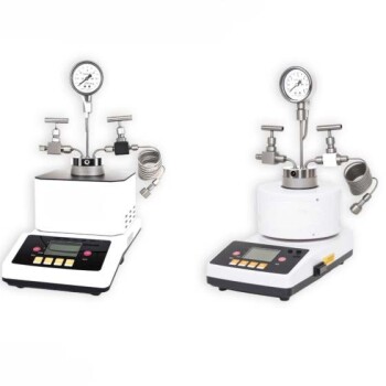
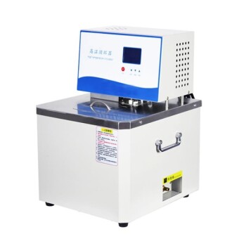
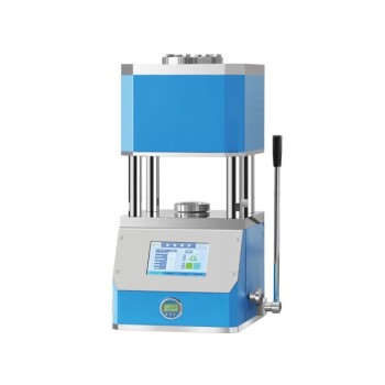
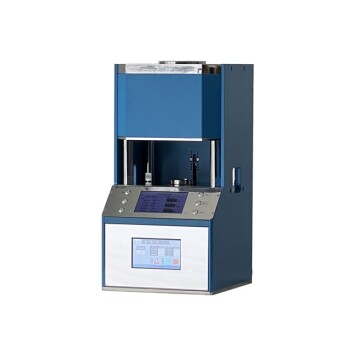
- HFCVD Machine System Equipment for Drawing Die Nano-Diamond Coating
- Chemical Vapor Deposition CVD Equipment System Chamber Slide PECVD Tube Furnace with Liquid Gasifier PECVD Machine
- Molybdenum Tungsten Tantalum Evaporation Boat for High Temperature Applications
- Microwave Plasma Chemical Vapor Deposition MPCVD Machine System Reactor for Lab and Diamond Growth
- Customer Made Versatile CVD Tube Furnace Chemical Vapor Deposition Chamber System Equipment
People Also Ask
- What is the chemical vapor deposition growth process? Build Superior Thin Films from the Atom Up
- What is the function of tungsten filaments in HFCVD? Powering Diamond Film Synthesis with Thermal Excitation
- Why is Chemical Vapor Deposition (CVD) equipment uniquely suited for constructing hierarchical superhydrophobic structures?
- What are the advantages of chemical vapor deposition? Achieve Superior Thin Films for Your Lab
- What are the disadvantages and challenges of the HFCVD method? Overcome Growth Limits and Filament Issues