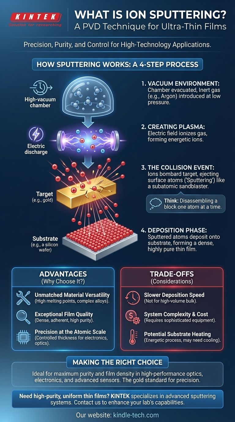
At its core, ion sputtering is a physical vapor deposition (PVD) technique used to create ultra-thin films with exceptional precision. The process takes place in a high-vacuum chamber where a target material is bombarded by energetic ions, typically from an inert gas like argon. This high-energy collision acts like a subatomic sandblaster, ejecting individual atoms from the target, which then travel and deposit onto a substrate, forming a dense, high-purity coating.
Think of sputtering not as painting a surface, but as disassembling a block of material one atom at a time and reassembling it flawlessly onto a new surface. It is the go-to method when precision, purity, and the ability to work with difficult materials are non-negotiable.
How Sputtering Works: A Step-by-Step Breakdown
To understand the value of sputtering, it's helpful to visualize the key stages of the process. Each step is meticulously controlled to ensure the final film meets exact specifications.
The Vacuum Environment
The entire process begins by creating a high vacuum inside a sealed chamber. This removes air and other potential contaminants that could otherwise get trapped in the thin film and compromise its quality. An inert gas, most commonly argon, is then introduced at very low pressure.
Creating the Plasma
An electric field is applied within the chamber, energizing the argon gas and stripping electrons from the argon atoms. This creates a plasma, an ionized gas consisting of positive argon ions and free electrons. This plasma is the source of the "ions" that will do the work.
The Collision Event
The target, which is made of the material you wish to deposit (e.g., gold, titanium, silicon dioxide), is given a negative electrical charge. This attracts the positively charged argon ions from the plasma, causing them to accelerate and collide with the target at high speed.
This bombardment has enough energy to knock atoms or molecules completely free from the target material. This ejection of surface atoms is the "sputtering" itself.
The Deposition Phase
The sputtered atoms travel in straight lines from the target until they strike a nearby object—the substrate. This is the component being coated, such as a semiconductor wafer, a lens, or a medical implant.
As millions of these atoms land on the substrate, they build up layer by layer, forming a thin, dense, and highly uniform film. The thickness can be controlled with extreme precision, often down to a few nanometers.
Key Applications and Advantages
Sputtering isn't chosen for its speed; it's chosen for its control and quality. This makes it indispensable in a range of high-technology fields.
Unmatched Material Versatility
Sputtering excels where other methods struggle. It is one of the few techniques that can reliably deposit materials with very high melting points, as well as complex alloys and compounds, while preserving their chemical composition.
Exceptional Film Quality
Because the sputtered atoms arrive at the substrate with significant energy, they form films that are incredibly dense and adhere strongly to the surface. The high-vacuum environment ensures exceptional purity, which is critical for optical and electronic performance.
Precision at the Atomic Scale
The process allows for meticulous control over film thickness and uniformity. This is why sputtering is essential for manufacturing:
- Semiconductors: Creating the microscopic metal layers that form integrated circuits.
- Precision Optics: Applying anti-reflective or reflective coatings to lenses and mirrors.
- Data Storage: Depositing the magnetic layers on hard disk drives and CDs.
- Advanced Sensors: Building components for devices like gyroscopes.
Understanding the Trade-offs
No process is perfect for every situation. Being a trusted advisor means acknowledging the limitations.
Deposition Speed
Sputtering is generally a slower process compared to other PVD techniques like thermal evaporation. The rate of material ejection is fundamentally limited by the ion bombardment physics, making it less suitable for high-volume, low-cost bulk coatings.
System Complexity and Cost
Achieving the necessary high vacuum and generating a stable plasma requires sophisticated and expensive equipment. The initial capital investment and ongoing maintenance for a sputtering system are significant.
Potential for Substrate Heating
The energetic particles (ions and sputtered atoms) can transfer a considerable amount of energy to the substrate, causing it to heat up. For heat-sensitive substrates, like certain plastics or biological samples, this requires careful management or cooling systems to prevent damage.
Making the Right Choice for Your Goal
Deciding on a deposition technique depends entirely on your project's technical and commercial requirements.
- If your primary focus is maximum purity and film density for high-performance optics or electronics: Ion sputtering is the superior choice due to its controlled energy and clean vacuum environment.
- If you need to deposit complex alloys or refractory metals with high melting points: Sputtering offers a reliable and repeatable path where methods like evaporation often fail.
- If your primary concern is high-speed, bulk deposition for less critical applications: You might consider other methods like thermal evaporation, which can be faster and more cost-effective.
Ultimately, ion sputtering empowers engineers to build with atomic-level precision, turning challenging materials into high-performance components.
Summary Table:
| Key Aspect | Description |
|---|---|
| Process | Physical Vapor Deposition (PVD) using ion bombardment. |
| Environment | High-vacuum chamber with inert gas (e.g., Argon). |
| Primary Advantage | Exceptional film purity, density, and material versatility. |
| Common Applications | Semiconductors, precision optics, data storage, sensors. |
| Main Limitation | Slower deposition speed compared to other PVD methods. |
Need a high-purity, uniform thin film for your project?
Ion sputtering is the gold standard for precision coating, but choosing the right equipment is critical for success. KINTEK specializes in advanced lab equipment and consumables for all your deposition needs. Our experts can help you select the ideal sputtering system to achieve the exceptional film quality and material versatility your research or production demands.
Contact us today to discuss how our solutions can enhance your laboratory's capabilities!
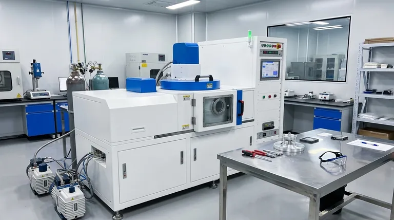
Visual Guide
Related Products
- Chemical Vapor Deposition CVD Equipment System Chamber Slide PECVD Tube Furnace with Liquid Gasifier PECVD Machine
- Customer Made Versatile CVD Tube Furnace Chemical Vapor Deposition Chamber System Equipment
- Inclined Rotary Plasma Enhanced Chemical Vapor Deposition PECVD Equipment Tube Furnace Machine
- Three-dimensional electromagnetic sieving instrument
- Spark Plasma Sintering Furnace SPS Furnace
People Also Ask
- Why is Chemical Vapor Deposition (CVD) equipment uniquely suited for constructing hierarchical superhydrophobic structures?
- What are the core advantages of PE-CVD in OLED encapsulation? Protect Sensitive Layers with Low-Temp Film Deposition
- How expensive is chemical vapor deposition? Understanding the True Cost of High-Performance Coating
- What are the processes of vapor phase deposition? Understand CVD vs. PVD for Superior Thin Films
- What happens during deposition chemistry? Building Thin Films from Gaseous Precursors


