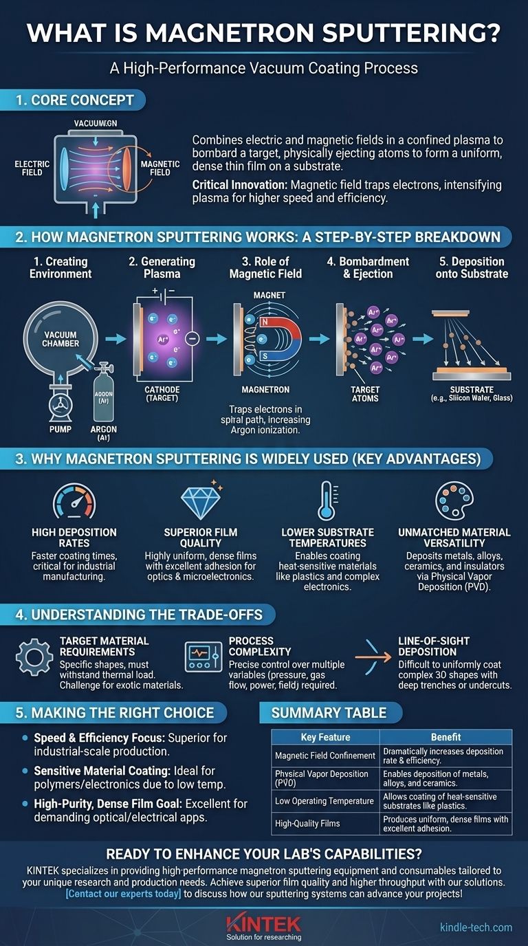
In essence, magnetron sputtering is a high-performance vacuum coating process. It uses a powerful combination of an electric and magnetic field to create a confined plasma. This plasma bombards a source material, known as a target, with ions, physically knocking atoms loose and depositing them as an exceptionally uniform and dense thin film onto a substrate.
The critical innovation of magnetron sputtering is its use of a magnetic field to trap electrons near the target material. This intensifies the plasma, dramatically increasing the efficiency and speed of the deposition process compared to older sputtering methods.
How Magnetron Sputtering Works: A Step-by-Step Breakdown
To understand why this technique is so effective, it's best to visualize the process in distinct stages. The entire operation takes place inside a sealed, low-pressure vacuum chamber.
Creating the Environment
First, the chamber is pumped down to a vacuum to remove contaminants. Then, it is backfilled with a small, controlled amount of an inert gas, most commonly Argon (Ar).
Generating the Plasma
A high negative voltage is applied to the target material, which acts as the cathode. This strong electric field causes the Argon gas to break down into a glowing plasma, consisting of positive Argon ions (Ar+) and free electrons.
The Role of the Magnetic Field
This is the "magnetron" part of the name. A permanent magnet or electromagnet is placed behind the target. This creates a magnetic field that is perpendicular to the electric field on the target's surface.
This magnetic field traps the much lighter electrons, forcing them into a spiral path near the target. This drastically increases the probability that an electron will collide with and ionize a neutral Argon atom, creating more Ar+ ions.
Bombardment and Ejection
The dense cloud of positively charged Ar+ ions is aggressively accelerated by the electric field toward the negatively charged target. These ions strike the target with high energy, physically knocking out, or "sputtering," atoms of the target material.
Deposition onto the Substrate
The ejected target atoms travel through the vacuum chamber and land on the substrate (such as a silicon wafer or a piece of glass), gradually building up a thin, even film.
Why Magnetron Sputtering is Widely Used
The unique mechanism of magnetron sputtering provides several significant advantages that have made it a cornerstone of industrial and research applications.
High Deposition Rates
By creating a much denser plasma right where it's needed, the magnetic field dramatically increases the rate of sputtering. This translates to faster coating times, which is critical for manufacturing.
Superior Film Quality
The process produces films that are highly uniform, dense, and have excellent adhesion to the substrate. This quality is essential for high-performance applications in optics and microelectronics.
Lower Substrate Temperatures
Compared to some other deposition techniques like thermal evaporation, magnetron sputtering can operate at much lower temperatures. This allows for the coating of heat-sensitive materials, including plastics and complex electronics.
Unmatched Material Versatility
The technique is a form of Physical Vapor Deposition (PVD), meaning it's based on a physical ejection mechanism, not a chemical or thermal one. This allows it to deposit a vast range of materials, including metals, alloys, ceramics, and even some insulating materials.
Understanding the Trade-offs
While powerful, the technique is not without its specific requirements and limitations. An objective assessment requires understanding these points.
Target Material Requirements
The source material must be fabricated into a specific target shape that can be installed in the equipment and withstand the thermal load from ion bombardment. This can sometimes be a manufacturing challenge for more exotic or brittle materials.
Process Complexity
Achieving a specific film thickness, composition, and crystal structure is not trivial. It requires precise control over multiple variables, including chamber pressure, gas flow, target power, and magnetic field geometry.
Line-of-Sight Deposition
Like most PVD processes, sputtering is a "line-of-sight" technique. Sputtered atoms travel in relatively straight lines, which can make it difficult to uniformly coat complex, three-dimensional shapes with deep trenches or undercuts.
Making the Right Choice for Your Goal
Selecting a deposition method depends entirely on the desired outcome. Magnetron sputtering excels in specific scenarios.
- If your primary focus is speed and efficiency: Magnetron sputtering is a superior choice for industrial-scale production due to its high deposition rates.
- If you are coating sensitive materials: The low deposition temperature makes it ideal for substrates like polymers or complex electronics that cannot withstand high heat.
- If your goal is a high-purity, dense film: The PVD nature of the process ensures excellent film quality for demanding optical or electrical applications.
Ultimately, understanding the role of the magnetic field is the key to appreciating why magnetron sputtering has become a foundational technology for modern thin-film engineering.
Summary Table:
| Key Feature | Benefit |
|---|---|
| Magnetic Field Confinement | Dramatically increases deposition rate and efficiency |
| Physical Vapor Deposition (PVD) | Enables deposition of metals, alloys, and ceramics |
| Low Operating Temperature | Allows coating of heat-sensitive substrates like plastics |
| High-Quality Films | Produces uniform, dense films with excellent adhesion |
Ready to enhance your lab's capabilities with precise thin-film deposition?
KINTEK specializes in providing high-performance magnetron sputtering equipment and consumables tailored to your laboratory's unique research and production needs. Our solutions help you achieve superior film quality, higher throughput, and the ability to work with sensitive materials.
Contact our experts today to discuss how our sputtering systems can advance your projects!
Visual Guide
Related Products
- Spark Plasma Sintering Furnace SPS Furnace
- RF PECVD System Radio Frequency Plasma-Enhanced Chemical Vapor Deposition RF PECVD
People Also Ask
- What is the mechanism of SPS process? A Deep Dive into Rapid, Low-Temperature Sintering
- What is the pressure for spark plasma sintering? A Guide to Optimizing SPS Parameters
- What is the process fundamentals of spark plasma sintering? Achieve Rapid, High-Density Material Consolidation
- What is SPS sintering method? A Guide to High-Speed, High-Performance Material Fabrication
- What is the theory of spark plasma sintering? A Guide to Rapid, Low-Temperature Densification

