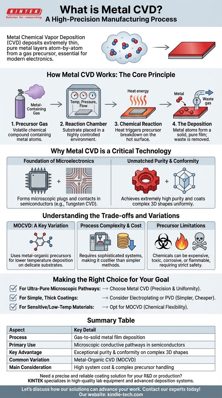
Metal Chemical Vapor Deposition (CVD) is a high-precision manufacturing process used to deposit extremely thin, pure layers of metal onto a surface. Rather than melting or shaping solid metal, this technique uses a metal-containing gas that chemically reacts in a controlled chamber, building a solid metal film one layer of atoms at a time. This method is fundamental to modern electronics, particularly in fabricating the microscopic conductive pathways inside semiconductor devices.
The core principle of Metal CVD is the transformation of a specialized, metal-containing gas (a precursor) into a solid, high-purity metal film on a target surface. This gas-to-solid conversion allows for the creation of intricate metallic structures that would be impossible to form using traditional methods.
How Metal CVD Works: The Core Principle
The process, while complex in practice, is based on a few straightforward physical and chemical principles. It all happens inside a highly controlled reaction chamber.
The Precursor Gas
The process begins with a "precursor," which is a chemical compound that contains the metal atoms we want to deposit. This precursor is designed to be volatile, meaning it exists as a gas at a relatively low temperature.
The Reaction Chamber
This precursor gas is introduced into a vacuum chamber containing the object to be coated, known as the substrate. The chamber's environment—temperature, pressure, and gas flow—is precisely controlled.
The Chemical Reaction
Energy, typically in the form of high heat, is applied to the substrate. When the precursor gas comes into contact with the hot surface, it triggers a chemical reaction.
The Deposition
This reaction breaks the precursor gas apart, freeing the metal atoms. These metal atoms then bond directly to the substrate's surface, forming a thin, solid, and exceptionally pure film of metal. The non-metallic components of the gas are pumped out as waste.
Why Metal CVD is a Critical Technology
While CVD is used for many materials, including synthetic diamonds, its application with metals is crucial for specific high-tech industries.
The Foundation of Microelectronics
The most significant application is in semiconductor manufacturing. Processes like Tungsten CVD are used to form the microscopic "plugs" and conductive contacts that connect the millions of transistors on a microchip. The precision of CVD is essential for building these complex, multi-layered structures.
Unmatched Purity and Conformity
Because the film is built from a gas, the resulting metal layer is extremely pure, which is vital for predictable electrical performance. Furthermore, the gas can penetrate and coat incredibly complex, three-dimensional shapes with a perfectly uniform layer, a feat many other coating techniques cannot achieve.
Understanding the Trade-offs and Variations
Metal CVD is a powerful tool, but it's not a universal solution. Understanding its limitations is key to appreciating its specific role.
MOCVD: A Key Variation
A common subset of this technology is Metal-Organic Chemical Vapor Deposition (MOCVD). This process uses metal-organic precursors, which often allows deposition to occur at lower temperatures, making it suitable for more delicate substrates.
Process Complexity and Cost
CVD systems are highly complex and expensive. They require sophisticated vacuum, temperature, and gas-flow controls, making the process much more costly than simpler coating methods.
Precursor Limitations
The precursor chemicals themselves can be a major consideration. They are often expensive, highly toxic, corrosive, or flammable, requiring stringent safety protocols and handling procedures.
Making the Right Choice for Your Goal
The decision to use Metal CVD depends entirely on the technical requirements of the final product.
- If your primary focus is creating ultra-pure, microscopic conductive pathways in electronics: Metal CVD, especially for metals like tungsten, is the industry standard due to its unmatched precision and uniformity.
- If your primary focus is coating a simple, flat object with a thick metal layer: Simpler, less expensive techniques like electroplating or Physical Vapor Deposition (PVD) are likely more suitable.
- If your primary focus is depositing a sensitive compound material or requires lower process temperatures: MOCVD is often the preferred method due to the greater flexibility of its precursor chemistry.
Understanding the principles of Metal CVD is key to appreciating how modern technology builds complex, powerful devices from the atom up.
Summary Table:
| Aspect | Key Detail |
|---|---|
| Process | Gas-to-solid deposition of metal films |
| Primary Use | Creating microscopic conductive pathways in semiconductors |
| Key Advantage | Exceptional purity and conformity on complex 3D shapes |
| Common Variation | Metal-Organic CVD (MOCVD) for lower-temperature processes |
| Main Consideration | High system cost and complex precursor handling |
Need a precise and reliable coating solution for your R&D or production?
Metal CVD is a cornerstone of modern microelectronics, and having the right equipment is critical for success. KINTEK specializes in high-quality lab equipment and consumables, including advanced deposition systems tailored for laboratory and pilot-scale applications. Our expertise ensures you get the precision and purity required for cutting-edge research and development.
Let's discuss how our solutions can advance your work. Contact our experts today for a personalized consultation!
Visual Guide
Related Products
- CVD Diamond for Thermal Management Applications
- Laboratory CVD Boron Doped Diamond Materials
- CVD Diamond Cutting Tool Blanks for Precision Machining
- CVD Diamond Dressing Tools for Precision Applications
- Custom CVD Diamond Coating for Lab Applications
People Also Ask
- Will a CVD diamond pass a diamond tester? Yes, because it's a real diamond.
- What are the optical properties of CVD diamond? Unlock Unmatched Performance for Demanding Applications
- What is the chemical vapour deposition method for diamonds? Grow a Diamond from a Gas
- Are CVD diamonds real or fake? Discover the Truth About Lab-Grown Diamonds
- What are the characteristics of CVD diamond? Unlocking Superior Performance for Industrial Tools