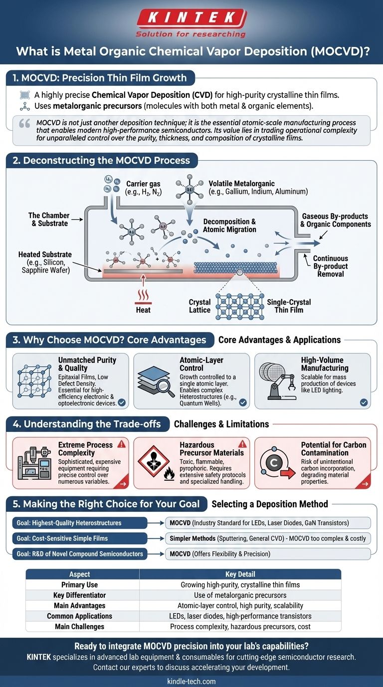
In short, Metal Organic Chemical Vapor Deposition (MOCVD) is a highly precise version of chemical vapor deposition (CVD) used to grow high-purity crystalline thin films. It is distinguished by its use of metalorganic precursors—specialized molecules containing both metal and organic elements—which are introduced into a reaction chamber to build materials layer by atomic layer on a substrate. This method is fundamental to manufacturing high-performance electronic and photonic devices, such as LEDs and lasers.
MOCVD is not just another deposition technique; it is the essential atomic-scale manufacturing process that enables modern high-performance semiconductors. Its value lies in trading operational complexity for unparalleled control over the purity, thickness, and composition of crystalline films.
Deconstructing the MOCVD Process
To understand MOCVD, it's best to break it down into its core components. The process is a sophisticated interplay between chemistry and physics inside a highly controlled environment.
The Reaction Chamber and Substrate
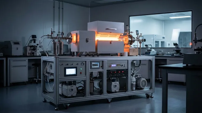
The entire process takes place inside a reaction chamber under vacuum. A substrate, which is the base material upon which the film will be grown (often a silicon or sapphire wafer), is placed inside and heated to a precise, elevated temperature.
The Precursors: The "Metal Organic" Heart
The key to MOCVD is the choice of precursor chemicals. These are metalorganic compounds, where a central metal atom (like Gallium, Indium, or Aluminum) is bonded to organic molecules.
These molecules are engineered to be volatile, meaning they easily turn into a gas. This allows them to be transported into the reaction chamber using a carrier gas, typically hydrogen or nitrogen.
Deposition and Film Growth
Once the gaseous metalorganic precursors flow over the hot substrate, they decompose in a chemical reaction. The organic part of the molecule breaks away, leaving the desired metal atoms on the surface.
These atoms migrate across the hot surface and settle into the most energetically favorable positions, arranging themselves into a perfect crystal lattice. This creates a single-crystal thin film that is an extension of the substrate's own crystal structure.
By-product Removal
The unwanted organic components and other reaction by-products remain in a gaseous state. They are continuously swept out of the reaction chamber by the gas flow, ensuring the deposited film remains exceptionally pure.
Why Choose MOCVD? Core Advantages
MOCVD is a dominant process in advanced manufacturing for several critical reasons, all stemming from its precision.
Unmatched Purity and Quality
The process yields epitaxial films, which are single-crystal layers with extremely low defect densities. This structural perfection is directly linked to the performance of electronic and optoelectronic devices, enabling higher efficiency and reliability.
Atomic-Layer Control
MOCVD allows for the growth of films with a thickness controlled down to a single atomic layer. By switching between different precursors, engineers can build complex, multi-layered structures called heterostructures, such as quantum wells, which are essential for modern lasers and LEDs.
High-Volume Manufacturing Scalability
While complex, MOCVD systems are designed for high-volume, reproducible manufacturing. Modern reactors can process multiple wafers simultaneously, making it commercially viable for mass-producing devices like LED lighting.
Understanding the Trade-offs
The precision of MOCVD comes with significant challenges that make it unsuitable for every application.
Extreme Process Complexity
MOCVD reactors are sophisticated and expensive pieces of equipment. Achieving high-quality results requires precise control over numerous variables, including temperature, pressure, gas flow rates, and chemical purity.
Hazardous Precursor Materials
The metalorganic precursors are often highly toxic, flammable, and pyrophoric (igniting spontaneously upon contact with air). Handling these materials necessitates extensive safety protocols, specialized facilities, and highly trained personnel.
Potential for Carbon Contamination
Because the precursors contain organic (carbon-based) molecules, there is a risk that carbon atoms can be unintentionally incorporated into the growing film. This contamination can degrade the electrical or optical properties of the final material.
Making the Right Choice for Your Goal
Selecting a deposition method depends entirely on balancing performance requirements with operational constraints.
- If your primary focus is creating the highest-quality semiconductor heterostructures: MOCVD is the industry standard and often the only viable choice for applications like high-brightness LEDs, laser diodes, and high-frequency GaN transistors.
- If your primary focus is cost-sensitive deposition of simple films: The cost, complexity, and safety overhead of MOCVD are likely excessive. Simpler methods like sputtering or general-purpose CVD might be more appropriate.
- If your primary focus is research and development of novel compound semiconductors: MOCVD offers the flexibility and precision needed to explore a vast range of material compositions and advanced device structures.
Ultimately, mastering MOCVD is the key to fabricating the foundational materials that power much of our advanced digital and illuminated world.
Summary Table:
| Aspect | Key Detail |
|---|---|
| Primary Use | Growing high-purity, crystalline thin films |
| Key Differentiator | Use of metalorganic precursors |
| Main Advantages | Atomic-layer control, high purity, scalability for manufacturing |
| Common Applications | LEDs, laser diodes, high-performance transistors |
| Main Challenges | Process complexity, hazardous precursors, cost |
Ready to integrate MOCVD precision into your lab's capabilities?
KINTEK specializes in providing the advanced lab equipment and consumables necessary for cutting-edge semiconductor research and production. Our expertise ensures you have the reliable tools and support to achieve unparalleled control over your thin film processes.
Contact our experts today to discuss how our solutions can accelerate your development of next-generation electronic and photonic devices.
Visual Guide
Related Products
- Chemical Vapor Deposition CVD Equipment System Chamber Slide PECVD Tube Furnace with Liquid Gasifier PECVD Machine
- Custom CVD Diamond Coating for Lab Applications
- CVD Diamond for Thermal Management Applications
- Customer Made Versatile CVD Tube Furnace Chemical Vapor Deposition Chamber System Equipment
- HFCVD Machine System Equipment for Drawing Die Nano-Diamond Coating
People Also Ask
- How expensive is chemical vapor deposition? Understanding the True Cost of High-Performance Coating
- What is the chemical vapor deposition growth process? Build Superior Thin Films from the Atom Up
- What are the core advantages of PE-CVD in OLED encapsulation? Protect Sensitive Layers with Low-Temp Film Deposition
- What are the processes of vapor phase deposition? Understand CVD vs. PVD for Superior Thin Films
- What is plasma enhanced chemical vapor deposition PECVD equipment? A Guide to Low-Temperature Thin Film Deposition


