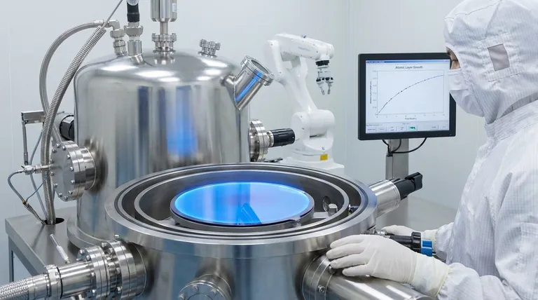
One of the most precise methods for depositing extremely controlled thin films is Atomic Layer Deposition (ALD). This technique builds material one atomic layer at a time through a sequence of self-limiting chemical reactions. This cyclic process gives engineers and scientists unparalleled, digital control over film thickness and composition, which is critical for manufacturing advanced semiconductors and nanotechnology.
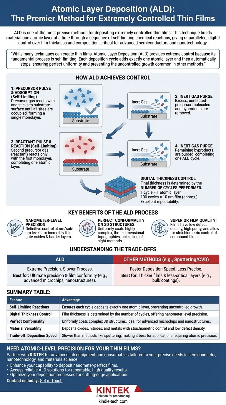
While many techniques can create thin films, Atomic Layer Deposition (ALD) provides extreme control because its fundamental process is self-limiting. Each deposition cycle adds exactly one atomic layer and then automatically stops, ensuring perfect uniformity and preventing the uncontrolled growth common in other methods.
How Atomic Layer Deposition Achieves Control
Atomic Layer Deposition is a specialized type of chemical vapor deposition (CVD). However, unlike traditional CVD where chemicals react continuously, ALD breaks the deposition down into a series of discrete, sequential steps.
The Self-Limiting Reaction Cycle
The core of ALD's precision lies in its two-part cycle, often called "half-reactions."
First, a precursor gas is pulsed into the chamber. The gas molecules react with and stick to the surface of the substrate until all available reactive sites are occupied. Because the molecules will not stick to each other, the reaction naturally stops after a single, complete monolayer is formed.
Next, the chamber is purged with an inert gas to remove any excess, unreacted precursor molecules.
Then, a second precursor gas (a reactant) is introduced. This gas reacts exclusively with the first monolayer, completing the deposition of a single, solid atomic layer of the desired material. This reaction is also self-limiting.
Finally, the chamber is purged again to remove any byproducts, completing one full ALD cycle.
Digital Control Over Thickness
Because each cycle dependably adds a single atomic layer, the final film thickness is determined simply by the number of cycles performed.
This provides a digital, rather than analog, method of control. If one cycle deposits 0.1 nanometers, then 100 cycles will deposit a 10-nanometer film with exceptional accuracy and excellent repeatability.
Perfect Conformality on 3D Structures
Since ALD relies on precursor gases that can penetrate microscopic features, it can deposit a perfectly uniform film over highly complex, three-dimensional topographies. This is a significant advantage over line-of-sight methods like sputtering, which struggle to evenly coat trenches and other advanced structures found in modern microchips.
Key Benefits of the ALD Process
The unique, self-limiting nature of ALD provides several key advantages for high-performance applications.
Nanometer-Level Precision
ALD offers definitive control of film thickness at the nanometer or even sub-nanometer level. This is essential for creating the incredibly thin gate oxides and barrier layers in cutting-edge transistors.
Superior Film Quality
The process results in films with low defect density and high purity. The precise, layer-by-layer growth also allows for stoichiometric control, meaning you can create compound films with an exact ratio of different elements.
Broad Material and Substrate Flexibility
ALD can be used to deposit a wide range of materials, including oxides, nitrides, and metals. Depending on the substrate and process temperature, it can produce either amorphous or crystalline films, adding to its versatility.
Understanding the Trade-offs
No technology is without its compromises. While ALD offers unmatched precision, its primary drawback must be considered.
The Primary Limitation: Deposition Speed
The cyclic, step-by-step nature of ALD makes it an inherently slow process. Each cycle can take from seconds to over a minute to complete.
Building a film that is tens of nanometers thick can be time-consuming compared to faster physical vapor deposition (PVD) methods like sputtering, which deposit material continuously.
When Other Methods Are Preferable
For applications that require thicker films (hundreds of nanometers or more) and do not demand atomic-level precision, methods like sputtering or conventional CVD are often more practical and cost-effective. These techniques offer much higher deposition rates, making them suitable for bulk coatings or less-critical layers.
Making the Right Choice for Your Application
Selecting a deposition technique requires aligning the method's capabilities with your project's most critical requirement.
- If your primary focus is ultimate precision and film conformity: ALD is the definitive choice for applications like advanced microchips or coating complex nanostructures where every atomic layer matters.
- If your primary focus is deposition speed for thicker or less-critical films: Consider faster methods like sputtering or conventional CVD, which are more economical when atomic-level control is not the priority.
Ultimately, selecting the right deposition method requires balancing the need for atomic precision against the practical demands of manufacturing speed and cost.
Summary Table:
| Feature | Advantage |
|---|---|
| Self-Limiting Reactions | Ensures each cycle deposits exactly one atomic layer, preventing uncontrolled growth. |
| Digital Thickness Control | Film thickness is determined by the number of cycles, offering nanometer-level precision. |
| Perfect Conformality | Uniformly coats complex 3D structures, ideal for advanced microchips and nanostructures. |
| Material Versatility | Deposits oxides, nitrides, and metals with stoichiometric control and low defect density. |
| Trade-off: Deposition Speed | Slower than methods like sputtering, making it best for applications requiring atomic precision. |
Need Atomic-Level Precision for Your Thin Films?
If your research or production demands the ultimate control over film thickness, uniformity, and conformality offered by Atomic Layer Deposition (ALD), KINTEK is here to help. We specialize in providing advanced lab equipment and consumables tailored to the precise needs of semiconductor, nanotechnology, and materials science laboratories.
Let us partner with you to:
- Enhance your capability to deposit nanometer-perfect films on complex structures.
- Access reliable ALD solutions that ensure repeatable, high-quality results.
- Optimize your deposition processes for cutting-edge applications.
Contact us today to discuss how our expertise can advance your projects: Get in Touch
Visual Guide
Related Products
- RF PECVD System Radio Frequency Plasma-Enhanced Chemical Vapor Deposition RF PECVD
- Chemical Vapor Deposition CVD Equipment System Chamber Slide PECVD Tube Furnace with Liquid Gasifier PECVD Machine
- HFCVD Machine System Equipment for Drawing Die Nano-Diamond Coating
- 915MHz MPCVD Diamond Machine Microwave Plasma Chemical Vapor Deposition System Reactor
- Inclined Rotary Plasma Enhanced Chemical Vapor Deposition PECVD Equipment Tube Furnace Machine
People Also Ask
- What is the role of RF-PECVD in VFG preparation? Mastering Vertical Growth and Surface Functionality
- What is plasma CVD? Unlock Low-Temperature Thin Film Deposition for Sensitive Materials
- What is plasma enhanced chemical vapour deposition process? Unlock Low-Temperature, High-Quality Thin Films
- What is plasma chemical vapor deposition? A Low-Temperature Thin Film Coating Solution
- Why is a Matching Network Indispensable in RF-PECVD for Siloxane Films? Ensure Stable Plasma and Uniform Deposition


