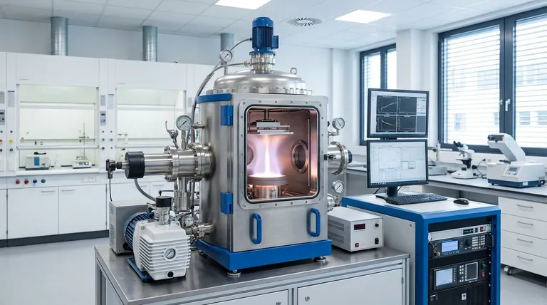
In crystal growth, Physical Vapor Deposition (PVD) is a family of vacuum-based techniques used to create high-purity, thin crystalline films. The core process involves physically transferring a material from a solid source (the "target") to a surface (the "substrate") on an atom-by-atom basis. This is accomplished by first converting the solid material into a vapor through methods like heating or ion bombardment, allowing the vapor to travel through a vacuum, and then letting it condense onto the substrate to form an ordered, crystalline structure.
The central challenge in growing perfect crystals is controlling how each atom arranges itself. PVD provides a direct physical pathway to achieve this, transforming a solid block of material into a flawless crystalline film without the need for complex chemical reactions.
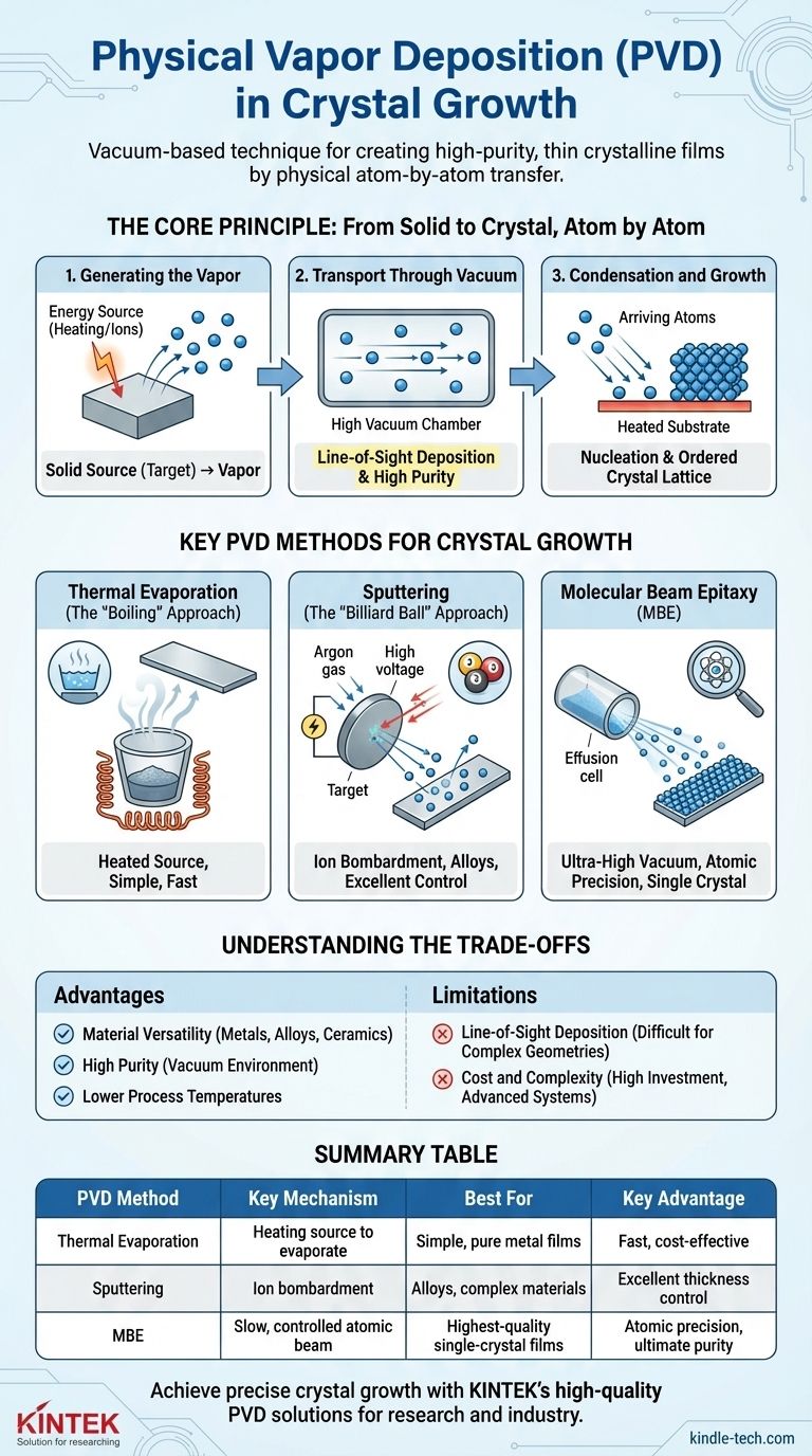
The Core Principle: From Solid to Crystal, Atom by Atom
PVD is fundamentally a process of physical transformation and controlled assembly. It can be broken down into three essential steps that occur within a high-vacuum chamber.
Step 1: Generating the Vapor
The process begins with a solid source material, known as a target. The goal is to liberate individual atoms or small clusters of atoms from this target. This is not achieved through chemical change, but through the input of physical energy.
Step 2: Transport Through Vacuum
Once freed, the vaporized atoms travel through a high-vacuum environment. The vacuum is critical for two reasons: it prevents the vaporized material from reacting with air, ensuring high film purity, and it allows the atoms to travel in a straight line to the substrate, a characteristic known as line-of-sight deposition.
Step 3: Condensation and Growth
When the atoms arrive at the substrate surface, they condense back into a solid state. For crystal growth, the substrate is typically heated. This gives the arriving atoms enough thermal energy to move around on the surface, find their lowest energy state, and lock into an ordered crystal lattice. This initial formation of tiny, ordered islands is called nucleation, which then serves as the foundation for the growing film.
Key PVD Methods for Crystal Growth
The "P" in PVD is broad, covering several distinct methods of vapor generation. The choice of method depends on the material being deposited and the desired quality of the crystal.
Thermal Evaporation (The "Boiling" Approach)
This is the simplest PVD method. The source material is placed in a crucible and heated by a resistive element until it evaporates, similar to how water boils into steam. The resulting vapor rises and condenses on the cooler substrate above. It's fast and effective for pure metals and simple compounds.
Sputtering (The "Billiard Ball" Approach)
In sputtering, the vacuum chamber is filled with a small amount of an inert gas, like Argon. A high voltage is applied, creating a plasma and accelerating the Argon ions toward the target. These energetic ions act like atomic-scale billiard balls, striking the target and knocking off atoms, which then deposit on the substrate. This method offers excellent control over film thickness and is ideal for depositing alloys and complex materials.
Molecular Beam Epitaxy (MBE)
MBE is the gold standard for achieving the highest-quality, single-crystal films. It operates under ultra-high vacuum conditions and uses an extremely slow deposition rate. The source material is heated gently in a specialized "effusion cell," producing a highly controlled beam of atoms. This allows for true layer-by-layer growth, enabling the creation of complex semiconductor structures with atomic precision.
Understanding the Trade-offs
No single technique is universally superior. The choice to use PVD, and which specific PVD method, involves clear trade-offs against other techniques like Chemical Vapor Deposition (CVD).
Advantage: Material Versatility and Purity
Because PVD is a physical process, it can be used to deposit almost any material that can be vaporized, including pure metals, alloys, and many ceramics. The vacuum environment ensures that the resulting film is exceptionally pure, as contamination from air is eliminated.
Advantage: Lower Process Temperatures
Many PVD processes can be run at significantly lower temperatures than their CVD counterparts. This is a major advantage when depositing films onto heat-sensitive substrates, such as plastics or pre-existing electronic devices.
Limitation: Line-of-Sight Deposition
The primary drawback of PVD is its directional nature. The vapor travels in a straight line from the source to the substrate, making it difficult to coat the surfaces of complex, three-dimensional objects uniformly. Gas-based methods like CVD are often better for coating intricate geometries.
Limitation: Cost and Complexity
While thermal evaporation can be relatively simple, more advanced PVD systems like sputtering and especially MBE are complex and expensive. Achieving the ultra-high vacuum and precise control required for high-quality crystal growth demands significant investment in equipment.
Making the Right Choice for Your Goal
The ideal PVD method is dictated entirely by your priorities for the final crystalline film.
- If your primary focus is ultimate purity and atomic-level control for research: Molecular Beam Epitaxy (MBE) is the unparalleled choice, despite its high cost and slow deposition rate.
- If your primary focus is depositing robust films of complex alloys or ceramics: Sputtering offers an excellent balance of control, uniformity, and reasonable throughput for industrial and research applications.
- If your primary focus is depositing simple, pure metal films quickly and cost-effectively: Thermal Evaporation is often the most practical and straightforward solution.
Ultimately, mastering PVD is about precisely controlling physical energy to guide atoms into forming a perfect crystalline structure.
Summary Table:
| PVD Method | Key Mechanism | Best For | Key Advantage |
|---|---|---|---|
| Thermal Evaporation | Heating source material to evaporate | Simple, pure metal films | Fast, cost-effective |
| Sputtering | Ion bombardment to knock off target atoms | Alloys, complex materials | Excellent thickness control |
| Molecular Beam Epitaxy (MBE) | Slow, controlled atomic beam | Highest-quality single-crystal films | Atomic precision, ultimate purity |
Ready to achieve precise crystal growth in your lab? KINTEK specializes in high-quality PVD equipment and consumables, from robust sputtering systems to advanced MBE solutions. Our expertise ensures you get the right tools for depositing high-purity, crystalline films—whether for research or industrial applications. Contact us today to enhance your lab's capabilities with tailored PVD solutions!
Visual Guide
Related Products
- Chemical Vapor Deposition CVD Equipment System Chamber Slide PECVD Tube Furnace with Liquid Gasifier PECVD Machine
- RF PECVD System Radio Frequency Plasma-Enhanced Chemical Vapor Deposition RF PECVD
- Customer Made Versatile CVD Tube Furnace Chemical Vapor Deposition Chamber System Equipment
- Microwave Plasma Chemical Vapor Deposition MPCVD Machine System Reactor for Lab and Diamond Growth
- Custom CVD Diamond Coating for Lab Applications
People Also Ask
- How are carbon nanotubes grown? Master Scalable Production with Chemical Vapor Deposition
- What are the core advantages of PE-CVD in OLED encapsulation? Protect Sensitive Layers with Low-Temp Film Deposition
- What are the processes of vapor phase deposition? Understand CVD vs. PVD for Superior Thin Films
- Why is Chemical Vapor Deposition (CVD) equipment uniquely suited for constructing hierarchical superhydrophobic structures?
- What is the chemical vapor deposition growth process? Build Superior Thin Films from the Atom Up


