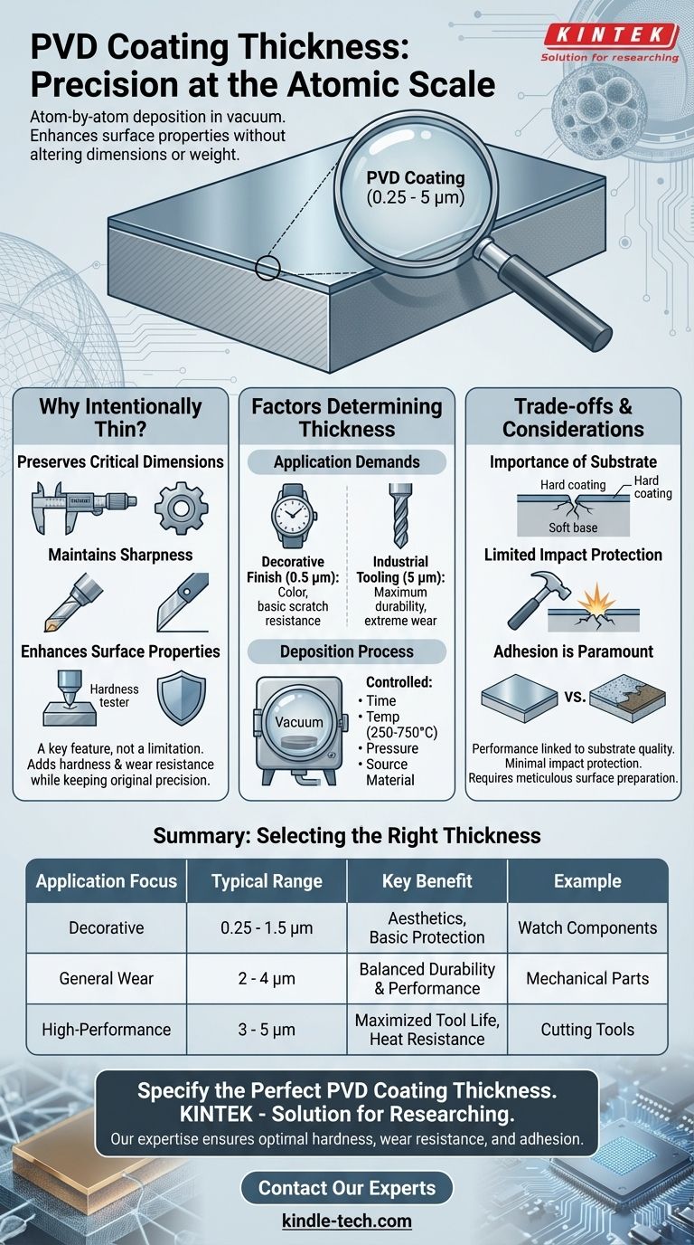
In short, PVD coating thickness is a precisely controlled parameter, typically ranging from 0.25 to 5 microns (µm). This is an incredibly thin film, applied atom-by-atom in a vacuum, designed to enhance the surface properties of a material without significantly altering its physical dimensions or weight.
The core principle of Physical Vapor Deposition (PVD) is that its extreme thinness is a deliberate feature, not a limitation. The goal is to add superior surface characteristics like hardness and wear resistance while preserving the substrate's original precision, sharpness, and core integrity.

Why PVD Coatings Are Intentionally Thin
The effectiveness of a PVD coating comes from its molecular bond with the substrate, creating a new, high-performance surface. Its minimal thickness is fundamental to how it achieves this.
Preserving Critical Dimensions
PVD is an atomistic deposition process, meaning it builds a coating one molecule at a time. This results in a film that is exceptionally uniform and thin.
For precision-engineered components, this is critical. A coating of just a few microns does not change the part's dimensional tolerances, ensuring it functions exactly as designed.
Maintaining Sharpness on Cutting Tools
A key application for PVD is on cutting tools like drills and end mills. A thicker coating would round the cutting edge, reducing its sharpness and effectiveness.
PVD coatings, often between 3 to 5 microns for these applications, are thin enough to maintain the original sharpness of the blade while adding significant hardness and wear resistance. This reduces cutting force and heat generation.
Enhancing Surface Properties, Not Bulk
The purpose of PVD is not to add material, but to change the characteristics of the existing surface.
It imparts properties like increased hardness, corrosion resistance, and reduced friction directly onto the substrate material, improving its performance and lifespan.
The Factors That Determine Coating Thickness
The final thickness of a PVD coating is not arbitrary; it is carefully engineered based on the specific requirements of the application.
The Application's Demands
Different uses require different thicknesses. A decorative finish on a watch might only need to be 0.5 microns thick to provide color and basic scratch resistance.
Conversely, a high-performance industrial tool subject to extreme wear may require a coating closer to 5 microns for maximum durability.
The Deposition Process
PVD is a physical process conducted in a vacuum at high temperatures, typically ranging from 250°C to 750°C.
The duration, temperature, pressure, and source material used during this process are all precisely controlled to achieve the desired coating composition and thickness.
Understanding the Trade-offs of Thin Films
While highly effective, it's important to understand the context in which these thin coatings operate. Their performance is directly linked to the quality of the underlying material.
The Importance of the Substrate
A PVD coating is only as strong as the foundation it's applied to. Its properties are determined by the underlying substrate material.
Applying an extremely hard coating to a soft substrate can lead to failure, as the base material may deform under load, causing the hard coating to crack or delaminate.
Limited Impact Protection
PVD coatings provide outstanding resistance to abrasive and sliding wear. However, their extreme thinness offers minimal protection against significant impacts.
A sharp, heavy impact can penetrate the coating and damage the substrate beneath it. The coating improves surface durability, not the part's overall impact strength.
Adhesion is Paramount
The bond between the coating and the substrate is critical. PVD offers excellent adhesion, but this is dependent on meticulous surface preparation.
If the surface is not perfectly clean and prepared, the coating will not bond correctly and can flake off, rendering it useless regardless of its thickness.
Selecting the Right Thickness for Your Application
Choosing the correct coating thickness is a balance between performance requirements, component function, and cost.
- If your primary focus is a decorative finish: A thinner coating (0.25 to 1.5 microns) is typically sufficient to provide the desired color, texture, and basic scratch resistance.
- If your primary focus is general wear resistance: A mid-range thickness (2 to 4 microns) offers a robust balance of durability and performance for most mechanical components.
- If your primary focus is high-performance cutting or tooling: A thicker coating (3 to 5 microns) is necessary to maximize tool life and heat resistance in demanding industrial environments.
Ultimately, PVD coating thickness is a critical design variable used to engineer a superior surface perfectly suited to its intended task.
Summary Table:
| Aspect | Typical Range | Key Detail |
|---|---|---|
| Thickness | 0.25 to 5 microns (µm) | Atom-by-atom deposition in a vacuum |
| Decorative Use | 0.25 to 1.5 µm | Provides color and basic scratch resistance |
| General Wear Resistance | 2 to 4 µm | Balances durability and performance |
| High-Performance Tooling | 3 to 5 µm | Maximizes tool life in demanding environments |
Need to specify the perfect PVD coating thickness for your components?
At KINTEK, we specialize in precision lab equipment and consumables for surface engineering. Our expertise ensures your PVD coatings deliver optimal hardness, wear resistance, and adhesion for your specific application—whether for cutting tools, decorative finishes, or industrial parts.
Contact our experts today to discuss how we can enhance your product's performance and longevity.
Visual Guide
Related Products
- RF PECVD System Radio Frequency Plasma-Enhanced Chemical Vapor Deposition RF PECVD
- Chemical Vapor Deposition CVD Equipment System Chamber Slide PECVD Tube Furnace with Liquid Gasifier PECVD Machine
- Split Chamber CVD Tube Furnace with Vacuum Station Chemical Vapor Deposition System Equipment Machine
- VHP Sterilization Equipment Hydrogen Peroxide H2O2 Space Sterilizer
- Molybdenum Tungsten Tantalum Special Shape Evaporation Boat
People Also Ask
- What is plasma activated chemical vapour deposition method? A Low-Temperature Solution for Advanced Coatings
- What is an example of PECVD? RF-PECVD for High-Quality Thin Film Deposition
- What are the benefits of PECVD? Achieve Superior Low-Temperature Thin Film Deposition
- Why does PECVD commonly use RF power input? For Precise Low-Temperature Thin Film Deposition
- What are the advantages of PECVD? Enable Low-Temperature, High-Quality Thin-Film Deposition