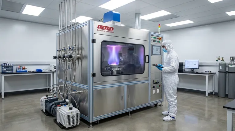
At its core, Physical Vapor Deposition (PVD) is a vacuum-based technique for applying extremely thin films of material onto a surface, or substrate. The process works by turning a solid source material into a vapor, which then travels through the vacuum and condenses onto the substrate, building the coating one atom at a time. This atomic-level control is what makes PVD a cornerstone of modern nanotechnology.
PVD is best understood not as a coating method, but as a form of "atomic spray painting" inside a high-vacuum chamber. It allows for the construction of ultra-pure, high-performance films with nanoscale precision, making it indispensable for creating advanced electronic and mechanical components.
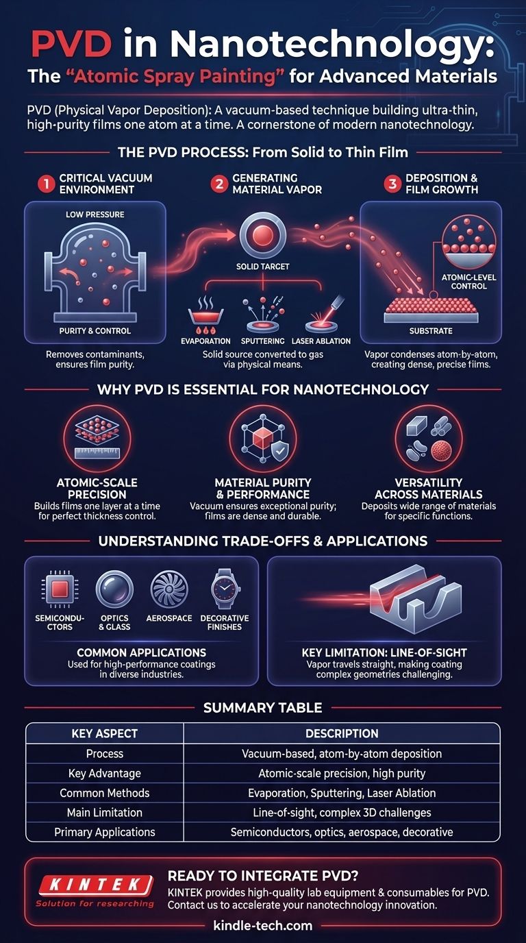
The PVD Process: From Solid to Thin Film
To understand PVD's role in nanotechnology, you must first grasp its fundamental mechanism. The entire process takes place under vacuum to ensure purity and control.
The Critical Vacuum Environment
The process is conducted at very low pressure, or high vacuum. This removes unwanted air and gas particles that could otherwise contaminate the film or interfere with the vaporized atoms as they travel to the substrate.
Generating the Material Vapor
A solid source material, known as the "target," is converted into a gas. This is achieved through purely physical means, such as:
- Evaporation: The target is heated until its atoms evaporate.
- Sputtering: The target is bombarded with high-energy ions, which knock atoms loose from its surface.
- Laser Ablation: A high-power laser vaporizes material from the target's surface.
Deposition and Film Growth
The vaporized atoms travel in a straight line through the vacuum chamber until they strike the cooler substrate. Upon contact, they condense back into a solid state, forming a thin, dense, and highly adherent film. Because this happens atom-by-atom, the resulting layer can be controlled with incredible precision.
Why PVD is Essential for Nanotechnology
PVD's unique characteristics make it perfectly suited for manufacturing on the nanoscale, where precision and purity are paramount. It is a physical process, meaning no chemical reactions occur, preserving the integrity of the deposited material.
Atomic-Scale Precision
The ability to build films one atomic layer at a time is the defining advantage of PVD. This level of control is necessary for creating components like semiconductors and thin-film solar panels, where layer thickness directly dictates electronic and optical properties.
Material Purity and Performance
Operating in a vacuum ensures the deposited film is exceptionally pure. This is critical for electronic applications where even tiny impurities can cause device failure. The resulting films are also dense and hard, improving a substrate's resistance to wear, high temperatures, and corrosion.
Versatility Across Materials
PVD is not limited to one type of material. It can be used to deposit a wide range of pure metals, alloys, non-metals, and compound films. This flexibility allows engineers to select the perfect material for a specific function, from creating conductive pathways in a microchip to applying a hard, decorative finish on jewelry.
Understanding the Trade-offs and Applications
While powerful, PVD is not a universal solution. Understanding its strengths and limitations is key to using it effectively.
Common Applications: From Microchips to Hardware
PVD is used across numerous industries for its ability to create high-performance thin films. Key applications include:
- Semiconductor Manufacturing: Creating the intricate layers of conductive and insulating materials in integrated circuits.
- Optics and Glass: Applying anti-reflective or reflective coatings on lenses and glass.
- Aerospace: Coating components to provide a barrier against high temperatures and wear.
- Decorative Finishes: Producing durable and brilliant metallic finishes on items like jewelry, watches, and household hardware.
Key Limitation: Line-of-Sight Deposition
A significant constraint of PVD is that it is a "line-of-sight" process. The vaporized atoms travel in a straight path from the target to the substrate. This means it can be difficult to uniformly coat complex, three-dimensional shapes with deep grooves or hidden surfaces.
Surface Finish Quality
PVD coatings precisely replicate the surface texture of the substrate they are applied to. A smooth, polished substrate will result in a smooth, lustrous PVD film, often eliminating the need for post-coating polishing to achieve a brilliant metallic finish.
Making the Right Choice for Your Goal
PVD is a highly specialized tool. Your final objective determines whether it is the correct approach for your project.
- If your primary focus is electronic or optical performance: PVD is the ideal method for creating the pure, uniform, and ultra-thin layers required for semiconductors, sensors, and advanced optics.
- If your primary focus is surface enhancement: Use PVD to create exceptionally durable, corrosion-resistant, or decorative coatings on tools, medical implants, and consumer products.
- If you are working with complex 3D geometries: Carefully evaluate whether PVD's line-of-sight nature can adequately cover all critical surfaces and consider alternative methods if necessary.
By controlling matter at the atomic level, PVD serves as a foundational tool for building the high-performance materials of the future.
Summary Table:
| Key Aspect | Description |
|---|---|
| Process | Vacuum-based technique to deposit thin films atom-by-atom. |
| Key Advantage | Atomic-scale precision and high material purity. |
| Common Methods | Evaporation, Sputtering, Laser Ablation. |
| Main Limitation | Line-of-sight deposition; challenges with complex 3D shapes. |
| Primary Applications | Semiconductors, optics, aerospace coatings, decorative finishes. |
Ready to integrate PVD technology into your lab's workflow?
KINTEK specializes in providing high-quality lab equipment and consumables for nanotechnology research and development. Whether you are developing next-generation semiconductors, advanced optical coatings, or durable surface enhancements, our expertise and solutions can help you achieve unparalleled precision and purity in your thin-film applications.
Contact us today via our contact form to discuss how our PVD systems and support can accelerate your innovation and enhance your lab's capabilities.
Visual Guide
Related Products
- RF PECVD System Radio Frequency Plasma-Enhanced Chemical Vapor Deposition RF PECVD
- Chemical Vapor Deposition CVD Equipment System Chamber Slide PECVD Tube Furnace with Liquid Gasifier PECVD Machine
- Split Chamber CVD Tube Furnace with Vacuum Station Chemical Vapor Deposition System Equipment Machine
- VHP Sterilization Equipment Hydrogen Peroxide H2O2 Space Sterilizer
- Molybdenum Tungsten Tantalum Special Shape Evaporation Boat
People Also Ask
- What is plasma activated chemical vapour deposition method? A Low-Temperature Solution for Advanced Coatings
- Why does PECVD commonly use RF power input? For Precise Low-Temperature Thin Film Deposition
- What is the principle of plasma enhanced chemical vapor deposition? Achieve Low-Temperature Thin Film Deposition
- What are the advantages of PECVD? Enable Low-Temperature, High-Quality Thin-Film Deposition
- What are the applications of PECVD? Essential for Semiconductors, MEMS, and Solar Cells


