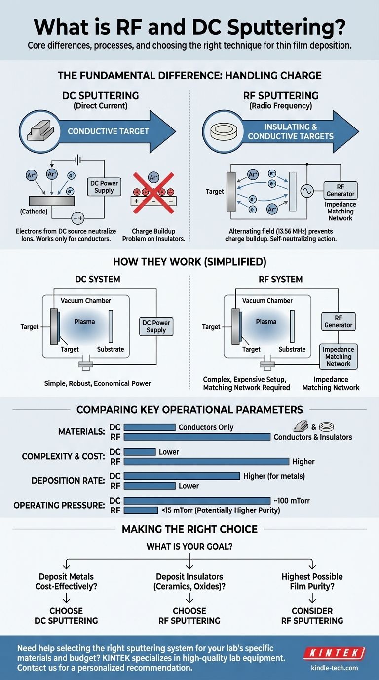
At its core, DC (Direct Current) sputtering is a cost-effective technique used to deposit thin films of electrically conductive materials, such as metals. In contrast, RF (Radio Frequency) sputtering is a more versatile method capable of depositing non-conductive, or insulating, materials like ceramics by using an alternating current to overcome technical limitations inherent in the DC process.
The fundamental choice between DC and RF sputtering comes down to the electrical properties of your target material. DC sputtering works only for conductors, while RF sputtering works for both conductors and insulators, solving the critical issue of electrical charge buildup on the target's surface.
The Fundamental Difference: Handling Electrical Charge
The primary distinction between these two physical vapor deposition (PVD) techniques lies in how they energize the target material to be deposited. This is dictated by the target's ability to conduct electricity.
How DC Sputtering Works
In a DC sputtering system, a high DC voltage is applied to a vacuum chamber. The target material, which is the source of the film, acts as the cathode (negative electrode).
A gas, typically Argon, is introduced and ionized, creating a plasma of positive ions and electrons. These positive ions are accelerated toward the negatively charged target, striking it with enough force to dislodge, or "sputter," atoms.
This process works efficiently as long as the target is electrically conductive. The constant flow of electrons from the DC power supply neutralizes the positive ions arriving at the target, allowing the process to continue.
The Charge Buildup Problem
If you attempt to use a non-conductive (insulating) target with a DC source, a problem called "charge buildup" occurs.
Positive ions still strike the target, but because the material is an insulator, the positive charge cannot be neutralized. The target surface quickly becomes positively charged, repelling the very ions needed to continue the sputtering process and effectively halting deposition.
The RF Sputtering Solution
RF sputtering solves the charge buildup problem by replacing the DC power source with a high-frequency AC power source, typically fixed at 13.56 MHz. This is in the radio frequency range, hence the name.
The rapid alternation of the electric field means the target is alternately bombarded by positive ions and electrons during each cycle. The electron bombardment phase effectively neutralizes the positive charge that builds up during the ion bombardment phase.
This "self-neutralizing" action prevents charge buildup, allowing for the continuous, stable sputtering of insulating materials. A special impedance-matching network is required to efficiently transfer the RF power to the plasma, making the system more complex than a DC setup.
Comparing Key Operational Parameters
Beyond the type of material, RF and DC sputtering differ in several important operational aspects that influence film quality, cost, and efficiency.
Power Source and Complexity
A DC sputtering system uses a simple, robust, and economical high-voltage DC power supply.
An RF sputtering system requires a more complex and expensive setup, including an RF generator and an impedance-matching network to manage the power transfer to the plasma.
System Pressure
DC sputtering typically operates at higher pressures (e.g., around 100 mTorr) to maintain a stable plasma.
RF sputtering can sustain a plasma at much lower pressures (e.g., under 15 mTorr). This is advantageous because fewer gas atoms in the chamber mean sputtered atoms are less likely to collide on their way to the substrate, resulting in a more direct deposition path and potentially higher-purity films.
Deposition Rate
For metals, DC sputtering generally offers a higher deposition rate and is more efficient.
RF sputtering typically has a lower sputter yield and deposition rate compared to DC sputtering for the same material, partly due to the energy consumed in the alternating electron and ion bombardment cycles.
Understanding the Trade-offs
Choosing a sputtering technique involves balancing capability against complexity and cost. Neither method is universally superior; they are tools designed for different tasks.
The Limitation of DC Sputtering: Materials
The single greatest drawback of DC sputtering is its inability to deposit dielectric (insulating) materials. This makes it unsuitable for applications involving many common ceramics, oxides, and polymers.
The Drawbacks of RF Sputtering: Cost and Rate
The primary trade-off for RF sputtering's versatility is its increased cost and complexity. The RF power supply and matching network are significantly more expensive than their DC counterparts.
Furthermore, the generally lower deposition rates can increase process time, impacting throughput, especially in large-scale production environments.
Making the Right Choice for Your Application
Your decision should be directly guided by the material you need to deposit and your project's budget and performance requirements.
- If your primary focus is depositing metals or other conductive materials cost-effectively: DC sputtering is the clear and standard choice for its simplicity, high deposition rate, and economic efficiency.
- If your primary focus is depositing insulating materials like ceramics or oxides: RF sputtering is the necessary and effective solution, as DC sputtering is not a viable option.
- If your primary focus is achieving the highest possible film purity and density: RF sputtering may offer an advantage even for some metals, as it can operate at lower pressures, reducing gas incorporation into the film.
Ultimately, understanding the electrical nature of your target material is the key to selecting the correct sputtering technology for your goal.
Summary Table:
| Feature | DC Sputtering | RF Sputtering |
|---|---|---|
| Best For | Conductive materials (metals) | Insulating & conductive materials (ceramics, oxides) |
| Complexity & Cost | Lower | Higher (requires RF generator & matching network) |
| Deposition Rate | Higher | Lower |
| Operating Pressure | Higher (~100 mTorr) | Lower (<15 mTorr) |
| Key Advantage | Cost-effective for metals | Can deposit insulating materials |
Need help selecting the right sputtering system for your lab's specific materials and budget?
At KINTEK, we specialize in providing high-quality lab equipment, including sputtering systems tailored for both conductive and insulating materials. Our experts can help you choose the perfect solution to achieve precise, high-purity thin films for your research or production needs.
Contact us today to discuss your application and get a personalized recommendation!
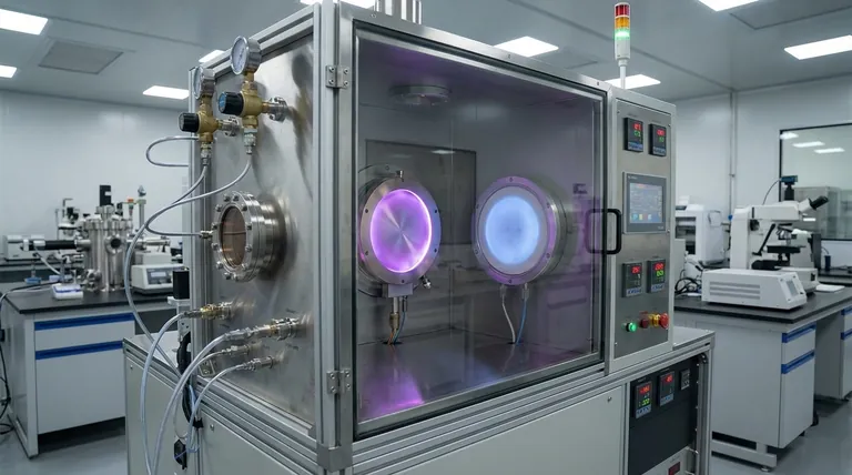
Visual Guide
Related Products
- Spark Plasma Sintering Furnace SPS Furnace
- Lab Sterile Slapping Type Homogenizer for Tissue Mashing and Dispersing
People Also Ask
- What is the process fundamentals of spark plasma sintering? Achieve Rapid, High-Density Material Consolidation
- What is SPS sintering method? A Guide to High-Speed, High-Performance Material Fabrication
- What is the difference between spark plasma sintering and flash sintering? A Guide to Advanced Sintering Methods
- What are the fundamentals of spark plasma sintering process? Unlock Rapid, High-Performance Material Consolidation
- Why are Spark Plasma Sintering (SPS) furnaces or hot presses utilized in the preparation of Li3PS4 solid electrolytes?

