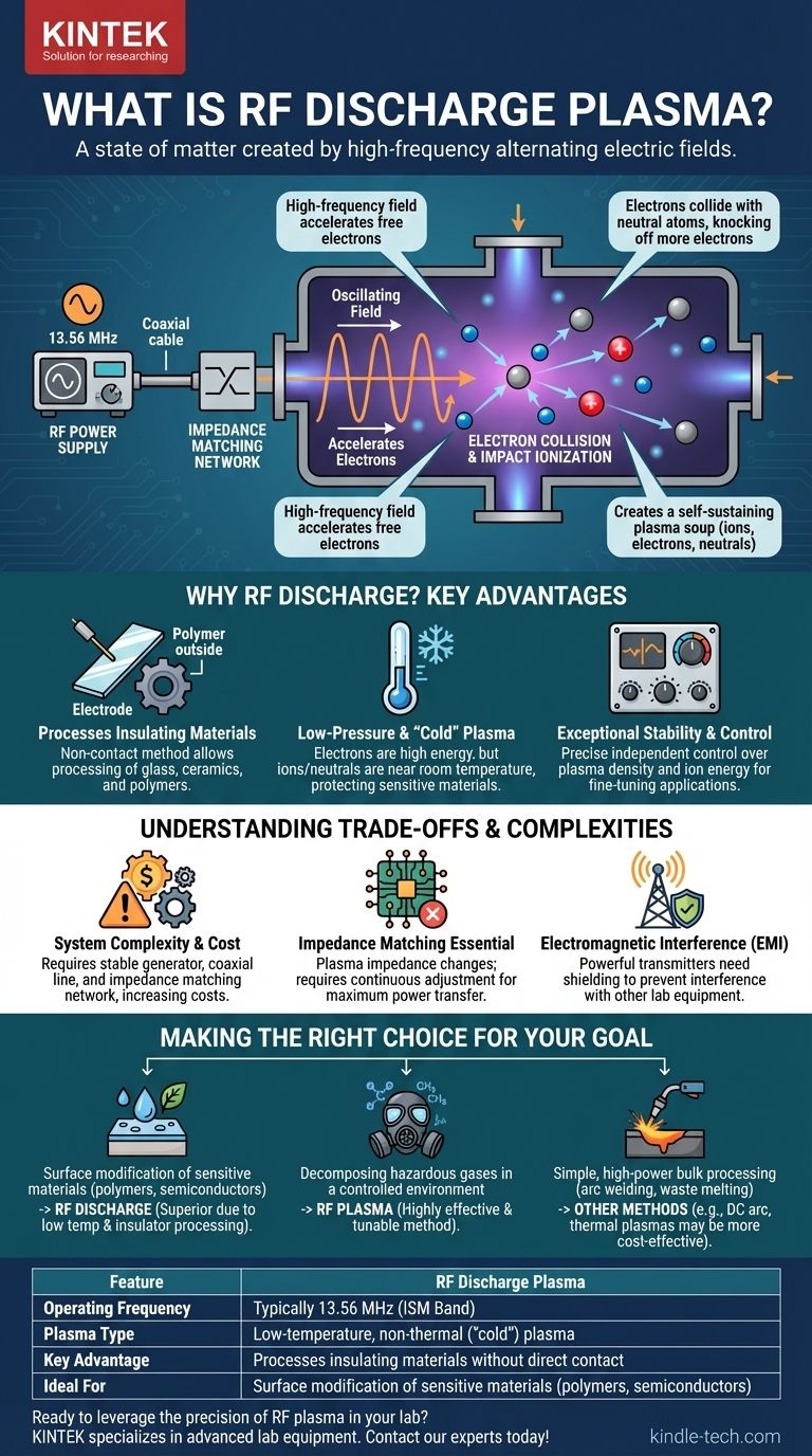
In essence, RF discharge plasma is a state of matter created when a gas is energized by a high-frequency alternating electric field, typically at a radio frequency (RF) like 13.56 MHz. This powerful field accelerates free electrons within the gas, causing them to collide with neutral atoms and knock off more electrons. This process creates a self-sustaining, highly reactive soup of ions, electrons, neutral atoms, and molecules known as plasma.
The core advantage of RF discharge is its ability to create stable, low-temperature ("cold") plasmas without direct electrode contact. This makes it an exceptionally precise and clean tool for processing sensitive materials that would be damaged by other methods.
How RF Fields Create Plasma
The generation of RF plasma is a precisely controlled chain reaction. It relies on the unique properties of an alternating electric field to pump energy into a low-pressure gas.
The Role of the Alternating Electric Field
Unlike a direct current (DC) field, which pushes electrons in one direction, an RF field oscillates millions of times per second. This oscillating field rapidly accelerates free electrons back and forth within the process chamber.
These electrons gain significant kinetic energy from the field but do not travel far before the field reverses, keeping them confined within the gas.
Electron Collision and Ionization
The high-energy electrons inevitably collide with neutral gas atoms. If an electron has enough energy, the collision will strip an electron from the neutral atom, creating a positive ion and another free electron.
This process, called impact ionization, is the fundamental mechanism for creating the plasma. The newly freed electron is also accelerated by the RF field, leading to more collisions in a cascade effect.
Achieving a Self-Sustaining Discharge
The plasma becomes stable, or "self-sustaining," when the rate of electron and ion creation is balanced by the rate at which they are lost, typically by recombining or hitting the chamber walls. The RF power supply continuously feeds energy into the system to maintain this equilibrium.
Why Use Radio Frequency? Key Advantages
RF discharge isn't the only way to make plasma, but its specific advantages have made it a cornerstone of high-tech industries.
Processing Insulating Materials
This is a critical advantage. Because the electric field is coupled capacitively or inductively (without direct contact), electrodes can be placed outside the reaction chamber. This allows RF plasma to process electrically insulating materials like glass, ceramics, and polymers, which is impossible with DC discharge.
Lower Pressure and Temperature Operation
RF discharges can be sustained at very low pressures. This low-pressure, high-energy electron environment creates what is known as a non-thermal or "cold" plasma.
In a cold plasma, the electrons are extremely hot (high energy), but the ions and neutral gas atoms remain near room temperature. This is crucial for modifying the surface of heat-sensitive materials like plastics or biological tissue without damaging them.
Exceptional Stability and Control
RF systems offer precise, independent control over plasma density and ion energy. By adjusting the RF power and gas pressure, operators can finely tune the chemical and physical properties of the plasma for a specific application, such as depositing a thin film with exact characteristics. The standard use of the 13.56 MHz frequency is regulated for industrial, scientific, and medical (ISM) use to prevent interference.
Understanding the Trade-offs
While powerful, RF plasma systems are not without their complexities and limitations.
System Complexity and Cost
An RF plasma system is more complex than a simple DC setup. It requires a stable RF power generator, a coaxial transmission line, and, most importantly, an impedance matching network. This increases the initial cost and maintenance requirements.
The Need for Impedance Matching
The plasma's electrical impedance (its resistance to the alternating current) changes dynamically as process conditions vary. An impedance matching network is a critical component that continuously adjusts the circuit to ensure maximum power is transferred from the generator to the plasma, not reflected back. Without proper matching, the process would be inefficient and could even damage the generator.
Electromagnetic Interference (EMI)
RF generators are essentially powerful radio transmitters. They must be properly shielded to prevent the strong electromagnetic fields from interfering with other sensitive lab or manufacturing equipment. This is a primary reason for the strict regulation of ISM frequencies.
Making the Right Choice for Your Goal
The decision to use RF discharge plasma depends entirely on the technical requirements of your specific application.
- If your primary focus is surface modification of sensitive materials (like polymers or semiconductors): RF discharge is often the superior choice due to its low-temperature operation and ability to process insulating materials.
- If your primary focus is decomposing hazardous gases in a controlled environment: RF plasma provides a highly effective and tunable method, as demonstrated in its early applications for breaking down fluorocarbons.
- If your primary focus is simple, high-power bulk processing (like arc welding or waste melting): Other methods like DC arc or thermal plasmas may be more cost-effective and straightforward for your needs.
Understanding the unique mechanism of RF discharge empowers you to select and optimize this powerful tool for advanced material science and industrial processing.
Summary Table:
| Feature | RF Discharge Plasma |
|---|---|
| Operating Frequency | Typically 13.56 MHz (ISM Band) |
| Plasma Type | Low-temperature, non-thermal ("cold") plasma |
| Key Advantage | Processes insulating materials without direct contact |
| Ideal For | Surface modification of sensitive materials (polymers, semiconductors) |
Ready to leverage the precision of RF plasma in your lab? KINTEK specializes in advanced lab equipment, including RF plasma systems, to help you achieve unparalleled surface modification and thin-film deposition. Our expertise ensures you get the right solution for processing sensitive materials like polymers and semiconductors. Contact our experts today to discuss your specific application needs!
Visual Guide
Related Products
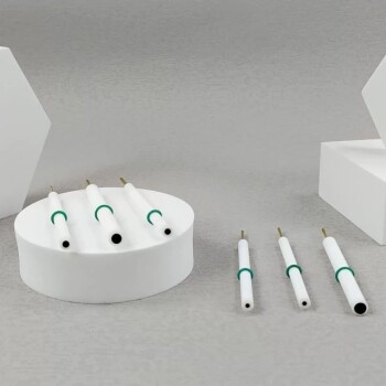
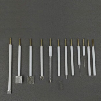
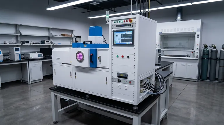
- RF PECVD System Radio Frequency Plasma-Enhanced Chemical Vapor Deposition RF PECVD
- Chemical Vapor Deposition CVD Equipment System Chamber Slide PECVD Tube Furnace with Liquid Gasifier PECVD Machine
- Microwave Plasma Chemical Vapor Deposition MPCVD Machine System Reactor for Lab and Diamond Growth
- Cylindrical Resonator MPCVD Machine System Reactor for Microwave Plasma Chemical Vapor Deposition and Lab Diamond Growth
- 10L Chilling Circulator Cooling Water Bath Low Temperature Constant Temperature Reaction Bath
People Also Ask
- How does RF power create plasma? Achieve Stable, High-Density Plasma for Your Applications
- What is plasma activated chemical vapour deposition method? A Low-Temperature Solution for Advanced Coatings
- What are the applications of PECVD? Essential for Semiconductors, MEMS, and Solar Cells
- How are PECVD and CVD different? A Guide to Choosing the Right Thin-Film Deposition Process
- What are the benefits of PECVD? Achieve Superior Low-Temperature Thin Film Deposition