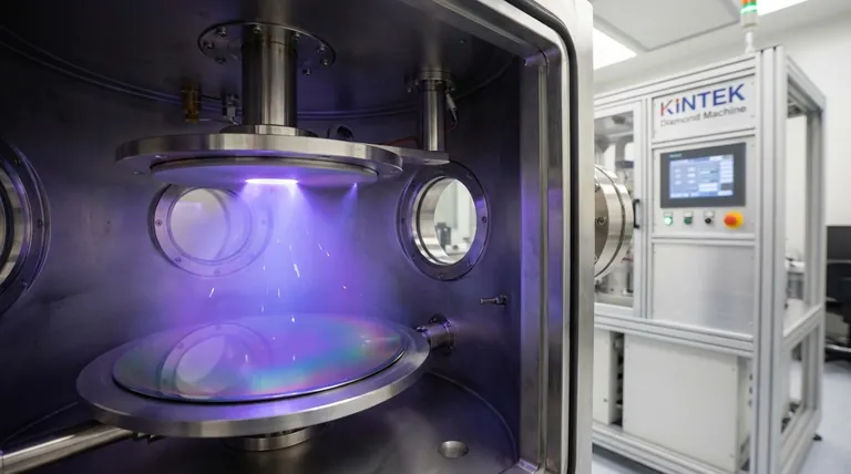
In engineering, sputtering is a physical vapor deposition (PVD) process used to create exceptionally thin, high-quality films of material onto a surface. It operates by ejecting atoms from a source material, known as a "target," by bombarding it with high-energy ions inside a vacuum. These ejected atoms then travel and deposit onto a nearby object, the "substrate," forming a uniform coating.
Sputtering is not a chemical reaction or a melting process; it is a physical momentum transfer. Think of it as a microscopic game of billiards where energetic ions are the cue ball, striking a rack of atoms (the target), and knocking some of them loose to coat a nearby surface.
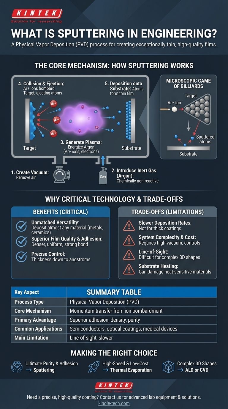
The Core Mechanism: How Sputtering Works
Sputtering is a highly controlled process that takes place within a sealed vacuum chamber. The fundamental steps are consistent regardless of the specific material being deposited.
Step 1: Creating a Vacuum
First, nearly all air is pumped out of the chamber to create a vacuum. This is critical to prevent the sputtered atoms from colliding with air molecules and to avoid contamination of the final film.
Step 2: Introducing an Inert Gas
A small, controlled amount of an inert gas, most commonly Argon (Ar), is then introduced into the chamber. This gas is chemically non-reactive and will be used to create the plasma.
Step 3: Generating a Plasma
A high voltage is applied within the chamber, creating a strong electric field. This field energizes the argon gas, stripping electrons from the argon atoms and creating a plasma—a glowing, ionized gas consisting of positive argon ions (Ar+) and free electrons.
Step 4: The Collision and Ejection
The material to be deposited, the target, is given a negative charge. This causes the positively charged argon ions from the plasma to accelerate violently towards it. These ions slam into the target with enough force to transfer their momentum, knocking individual atoms or molecules of the target material loose. This ejection process is the "sputtering" itself.
Step 5: Deposition onto the Substrate
The ejected target atoms travel through the vacuum chamber and land on the substrate (the object being coated), which is strategically placed nearby. As these atoms accumulate, they build up layer by layer, forming a thin, dense, and highly adherent film.
Why Sputtering Is a Critical Technology
Sputtering is chosen over other deposition methods when the quality, purity, and adhesion of the thin film are paramount. Its advantages make it indispensable in high-performance applications.
Unmatched Versatility
Virtually any material can be deposited via sputtering. This includes pure metals, complex alloys, and even insulating ceramic compounds like oxides and nitrides, which are difficult or impossible to deposit using other methods like thermal evaporation.
Superior Film Quality and Adhesion
Sputtered atoms arrive at the substrate with significantly more kinetic energy than evaporated atoms. This high energy promotes better surface mobility, resulting in denser, more uniform films with fewer defects. It also embeds the atoms slightly into the substrate surface, creating exceptionally strong adhesion.
Precise Control Over Thickness
The process is extremely stable and repeatable, allowing for precise control over the film's thickness and composition. Engineers can create films with thicknesses controlled down to a single angstrom (one ten-billionth of a meter).
Understanding the Trade-offs
Despite its powerful advantages, sputtering is not the ideal solution for every situation. It's essential to understand its limitations.
Slower Deposition Rates
Generally, sputtering is a slower process compared to methods like thermal evaporation. This makes it less economical for applications requiring very thick coatings (many microns).
System Complexity and Cost
Sputtering systems require high-vacuum pumps, sophisticated power supplies, and process controls. This makes the equipment more complex and expensive to purchase and maintain than simpler deposition systems.
Line-of-Sight Limitations
Like a spray paint can, sputtering is a line-of-sight process. The sputtered material travels in a straight line from the target to the substrate, making it difficult to uniformly coat complex, three-dimensional shapes with undercuts or hidden surfaces.
Potential for Substrate Heating
The energy transfer from the plasma and condensing atoms can significantly heat the substrate. While sometimes beneficial, this can damage heat-sensitive substrates like plastics or certain electronic components.
Making the Right Choice for Your Goal
Selecting a deposition method depends entirely on the specific requirements of your final product.
- If your primary focus is ultimate film purity, density, and adhesion for a complex material: Sputtering is often the superior technical choice.
- If your primary focus is high-speed, low-cost deposition of a simple metal: A process like thermal evaporation might be more efficient.
- If your primary focus is coating complex 3D shapes uniformly: You may need to explore non-line-of-sight methods like atomic layer deposition (ALD) or chemical vapor deposition (CVD).
Ultimately, understanding the principles of sputtering empowers you to select the precise manufacturing process for creating high-performance, durable surfaces.
Summary Table:
| Key Aspect | Description |
|---|---|
| Process Type | Physical Vapor Deposition (PVD) |
| Core Mechanism | Momentum transfer from ion bombardment (e.g., Argon) to a target material |
| Primary Advantage | Superior film adhesion, density, and purity for complex materials |
| Common Applications | Semiconductor manufacturing, optical coatings, medical devices |
| Main Limitation | Line-of-sight process; slower for thick coatings |
Need a precise, high-quality coating for your project? The sputtering process is ideal for applications demanding exceptional film purity, adhesion, and uniformity. KINTEK specializes in advanced lab equipment and consumables for thin film deposition, serving R&D and production labs. Let our experts help you select the right sputtering solution to enhance your product's performance and durability. Contact us today to discuss your specific coating requirements!
Visual Guide
Related Products
- Spark Plasma Sintering Furnace SPS Furnace
- Vacuum Induction Melting Spinning System Arc Melting Furnace
- Chemical Vapor Deposition CVD Equipment System Chamber Slide PECVD Tube Furnace with Liquid Gasifier PECVD Machine
- Customer Made Versatile CVD Tube Furnace Chemical Vapor Deposition Chamber System Equipment
People Also Ask
- What is the process fundamentals of spark plasma sintering? Achieve Rapid, High-Density Material Consolidation
- What is the pressure for spark plasma sintering? A Guide to Optimizing SPS Parameters
- What technical advantages does a Spark Plasma Sintering (SPS) furnace offer for LZP ceramics? Enhance Ionic Conductivity
- Why are Spark Plasma Sintering (SPS) furnaces or hot presses utilized in the preparation of Li3PS4 solid electrolytes?
- What is SPS sintering method? A Guide to High-Speed, High-Performance Material Fabrication


