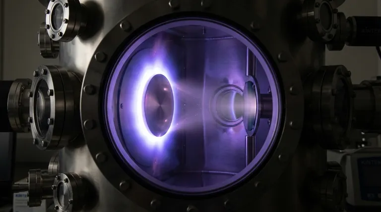
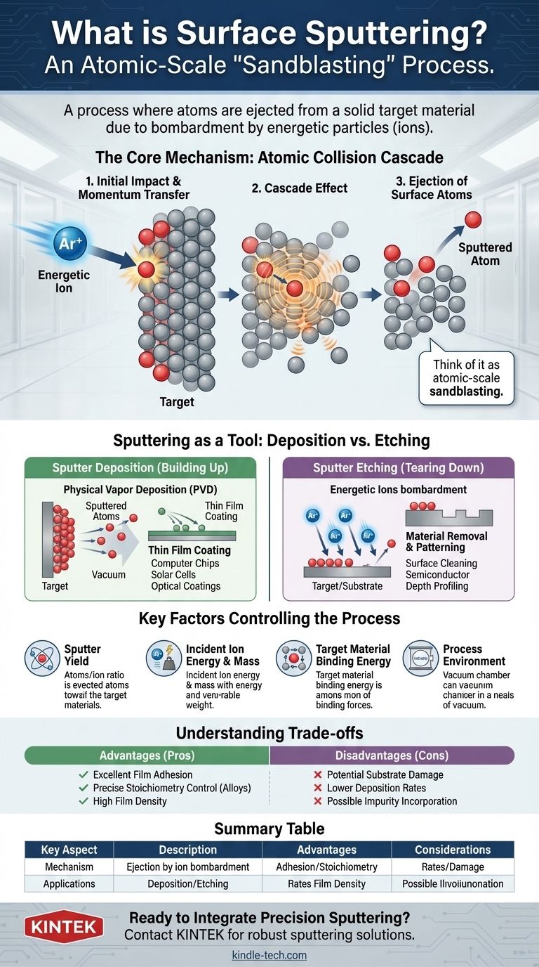
In materials science and physics, surface sputtering is a process where atoms are ejected from a solid target material due to bombardment by energetic particles, typically ions from a plasma. Think of it as a form of "sandblasting" on an atomic scale. An incoming high-energy ion strikes the target, initiating a cascade of collisions within the material that ultimately gives a surface atom enough energy to be knocked loose and fly away.
At its core, sputtering is not a random destructive effect but a highly controllable physical phenomenon. It is the fundamental mechanism behind two critical technologies: adding material layer-by-layer (sputter deposition) and precisely removing material (sputter etching).
The Core Mechanism: An Atomic Collision Cascade
To truly understand sputtering, you must visualize what happens when a single energetic ion hits a surface. The process is not a simple one-to-one exchange.
The Initial Impact
It begins when a high-energy ion, often an inert gas like Argon (Ar+), is accelerated and strikes the surface of a target material. These ions are generated in a low-pressure plasma environment.
Transfer of Momentum
Upon impact, the ion does not simply bounce off. Instead, it transfers its kinetic energy and momentum to the atoms within the target material, similar to a cue ball striking a tightly packed rack of billiard balls.
The Cascade Effect
This initial collision sets off a chain reaction, or collision cascade, deep within the material. The struck atom collides with its neighbors, which in turn collide with theirs. Energy is distributed through the crystal lattice in a series of rapid, atomic-scale impacts.
Ejection of Surface Atoms
If this collision cascade works its way back to the surface, and an atom at the surface receives enough momentum in an outward direction to overcome the material's binding energy, it is ejected. This ejected atom is the "sputtered" particle.
Sputtering as a Tool: Deposition vs. Etching
The true power of sputtering comes from harnessing the ejected atoms. Depending on the goal, it is used for either building up or tearing down material.
Sputter Deposition (Building Up)
In this primary application, a substrate (the object to be coated) is placed near the target. The atoms sputtered from the target travel through the vacuum and condense onto the substrate, forming a thin, uniform film.
This method, known as Physical Vapor Deposition (PVD), is critical for manufacturing everything from computer chips and solar cells to anti-reflective coatings on eyeglasses.
Sputter Etching (Tearing Down)
Alternatively, the goal can be to remove material from the substrate itself. In this case, the substrate is the target. Sputtering is used to clean surfaces at an atomic level or to precisely carve patterns into a material, a common step in semiconductor fabrication.
Key Factors Controlling the Sputtering Process
The efficiency and outcome of sputtering are not random. They are governed by several key parameters that engineers carefully control.
Sputter Yield
The single most important metric is the sputter yield: the average number of target atoms ejected per incident ion.
The Incident Ion
The "bullet" matters. The ion's energy is a primary control knob—higher energy generally leads to a higher sputter yield. The ion's mass is also critical; heavier ions like Argon or Krypton are more efficient at transferring momentum than lighter ones like Helium.
The Target Material
The "wall" matters, too. Materials with lower atomic binding energies—where atoms are less tightly held in place—are easier to sputter and thus have a higher sputter yield.
The Process Environment
Sputtering is performed in a high vacuum to ensure the sputtered atoms can travel from the target to the substrate without colliding with unwanted air molecules, which would contaminate the resulting film.
Understanding the Trade-offs and Consequences
While powerful, sputtering is a high-energy process with specific advantages and disadvantages that must be considered.
Advantage: Film Quality and Adhesion
Sputtered atoms arrive at the substrate with significantly higher kinetic energy than atoms from thermal evaporation. This energy helps them form a denser, more adherent film, which is crucial for durable coatings.
Advantage: Stoichiometry Control
Sputtering is excellent for depositing complex materials (alloys or compounds) because the process tends to remove atoms from the target in the same ratio they exist. This preserves the material's chemical composition, or stoichiometry, in the final film.
Disadvantage: Potential for Damage
The same high-energy ion bombardment that provides benefits can also be a drawback. It can introduce defects, stress, or unwanted embedded ions (like Argon) into the growing film or the substrate, potentially altering their electrical or optical properties.
Disadvantage: Lower Deposition Rates
Generally, sputtering is a slower deposition process compared to thermal evaporation. This makes it less ideal for applications requiring very thick films where speed is the primary concern.
Applying Sputtering to Your Goal
Your approach to sputtering should be dictated entirely by your end objective, whether you are creating a new material or analyzing an existing one.
- If your primary focus is creating high-performance thin films: Sputtering is your tool for achieving dense, adherent, and stoichiometrically precise coatings, especially for complex alloys, oxides, or nitrides.
- If your primary focus is surface cleaning or patterning: Sputter etching provides a highly directional and controlled method for removing material, but you must carefully manage ion energy to minimize damage to the underlying substrate.
- If your primary focus is surface analysis (e.g., SIMS or XPS): Sputtering is the mechanism used to perform depth profiling, removing one atomic layer at a time to reveal the composition underneath. Acknowledge that the ion beam itself can alter the chemistry you are trying to measure.
By moving beyond the simple definition, you can leverage sputtering as a precise and powerful instrument for engineering materials at the atomic scale.
Summary Table:
| Key Aspect | Description |
|---|---|
| Primary Mechanism | Ejection of target atoms via energetic ion bombardment (e.g., Ar+). |
| Main Applications | Sputter Deposition (thin films), Sputter Etching (material removal). |
| Key Advantages | Excellent film adhesion, precise stoichiometry control for alloys/compounds. |
| Key Considerations | Lower deposition rates vs. evaporation, potential for ion-induced substrate damage. |
Ready to Integrate Precision Sputtering into Your Lab Workflow?
Sputtering is essential for creating high-quality thin films and performing precise surface etching. KINTEK specializes in providing robust sputtering equipment and consumables tailored to your laboratory's specific research and production needs. Whether you are developing advanced semiconductors, optical coatings, or performing critical surface analysis, our expertise ensures you achieve superior results with excellent adhesion and stoichiometric control.
Contact KINTEK today to discuss how our sputtering solutions can enhance your material engineering processes.
Visual Guide
Related Products
- Spark Plasma Sintering Furnace SPS Furnace
- Vacuum Induction Melting Spinning System Arc Melting Furnace
- Chemical Vapor Deposition CVD Equipment System Chamber Slide PECVD Tube Furnace with Liquid Gasifier PECVD Machine
- Customer Made Versatile CVD Tube Furnace Chemical Vapor Deposition Chamber System Equipment
- Vacuum Cold Mounting Machine for Sample Preparation
People Also Ask
- What is the process fundamentals of spark plasma sintering? Achieve Rapid, High-Density Material Consolidation
- Why are Spark Plasma Sintering (SPS) furnaces or hot presses utilized in the preparation of Li3PS4 solid electrolytes?
- What is the difference between spark plasma sintering and flash sintering? A Guide to Advanced Sintering Methods
- What is the mechanism of SPS process? A Deep Dive into Rapid, Low-Temperature Sintering
- What is SPS sintering method? A Guide to High-Speed, High-Performance Material Fabrication


