The primary advantage of Chemical Vapor Deposition (CVD) is its exceptional ability to produce highly pure, dense, and uniform coatings that conform perfectly to complex surfaces. This "non-line of sight" capability, combined with its versatility in depositing a wide range of materials, makes it a uniquely powerful tool for creating high-performance thin films.
The core strength of CVD is not just that it deposits a layer, but that it grows a highly controlled film from a chemical reaction. This process results in coatings with superior purity, adhesion, and uniformity, especially on intricate shapes that are impossible to coat with line-of-sight methods.

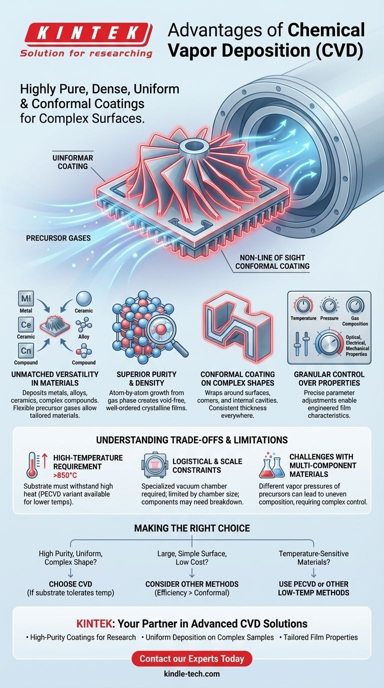
The Core Strengths of CVD Explained
To understand why CVD is chosen for demanding applications, we must look at how its fundamental process creates distinct advantages over other coating techniques.
Unmatched Versatility in Materials
CVD is not limited to a single class of material. The process is incredibly flexible, capable of depositing everything from metals and alloys to non-metal films, ceramics, and complex compounds.
This versatility stems from the wide variety of precursor gases that can be used, allowing engineers to tailor the coating material to the specific needs of the application.
Superior Purity and Density
The deposition process occurs through a chemical reaction of precursor gases directly on the substrate surface. This method inherently produces films of very high purity and density.
Because the material is built up atom by atom from a gaseous state, the resulting film is typically free of voids and has a well-ordered crystalline structure, which contributes to its durability and performance.
Conformal Coating on Complex Shapes
Perhaps the most significant advantage is CVD's non-line of sight nature. The precursor gases flow around the substrate, reaching every exposed surface, including internal cavities, sharp corners, and complex geometries.
This results in a "wrap-around" effect, creating a completely uniform coating of a consistent thickness, a feat that is difficult or impossible for methods like sputtering, which require a direct path from the source to the substrate.
Granular Control Over Film Properties
The final properties of the coating are not fixed. By precisely adjusting deposition parameters—such as temperature, pressure, and gas composition—operators can control the film's chemical makeup, crystal structure, and grain size.
This level of control allows for the engineering of films with specific optical, electrical, or mechanical properties.
Understanding the Trade-offs and Limitations
No process is without its challenges. An objective assessment of CVD requires understanding its operational constraints, which are critical for determining its suitability for a given project.
The High-Temperature Requirement
Traditional CVD processes operate at very high temperatures, often between 850°C and 1100°C. This heat is necessary to drive the chemical reactions that form the film.
This can be a major limitation, as many substrate materials cannot withstand such temperatures without deforming or degrading. However, variants like Plasma-Enhanced CVD (PECVD) have been developed to operate at much lower temperatures.
Logistical and Scale Constraints
CVD is typically performed in a specialized vacuum chamber at a dedicated coating center, meaning it cannot be done on-site. Parts must often be broken down into individual components before being coated.
Furthermore, the size of the vacuum chamber places a physical limit on the dimensions of the object that can be processed.
Challenges with Multi-Component Materials
While versatile, creating films from multiple components (alloys) can be difficult. Different precursor gases have different vapor pressures and reaction rates.
This can lead to a heterogeneous or uneven composition in the final film, requiring complex process control to achieve the desired material blend.
Making the Right Choice for Your Goal
Selecting the right coating technology depends entirely on your project's specific priorities and constraints.
- If your primary focus is achieving the highest possible purity and a perfectly uniform coating on a complex shape: CVD is an exceptional choice, provided your substrate can tolerate the process temperature.
- If your primary focus is coating a large, simple surface at low cost: Other methods might be more efficient, as CVD's strength in conformal coating is not the key requirement.
- If your primary focus is coating temperature-sensitive materials like plastics or certain alloys: You must specify a lower-temperature variant like PECVD or acknowledge that traditional CVD is not a viable option.
By understanding its unique strengths and inherent limitations, you can leverage Chemical Vapor Deposition to create advanced materials with precisely engineered properties.
Summary Table:
| Key Advantage | Description |
|---|---|
| Versatile Materials | Deposits metals, alloys, ceramics, and compounds with tailored properties |
| High Purity & Density | Produces void-free, crystalline films through controlled chemical reactions |
| Conformal Coating | Uniformly coats complex shapes, internal cavities, and sharp corners |
| Precise Control | Adjustable parameters for custom optical, electrical, and mechanical properties |
| Non-Line-of-Sight | Wraps around all exposed surfaces without direct source-to-substrate path |
Ready to enhance your materials with superior thin-film coatings?
At KINTEK, we specialize in advanced lab equipment and consumables for precise deposition processes. Our CVD solutions help laboratories achieve:
- High-purity coatings for critical research applications
- Uniform deposition on complex sample geometries
- Tailored film properties for specific material requirements
Whether you're working with metals, ceramics, or complex compounds, our expertise in laboratory equipment ensures you get the precise control and reliability your research demands.
Contact our experts today to discuss how our CVD solutions can advance your materials research and development.
Visual Guide
Related Products
- Chemical Vapor Deposition CVD Equipment System Chamber Slide PECVD Tube Furnace with Liquid Gasifier PECVD Machine
- RF PECVD System Radio Frequency Plasma-Enhanced Chemical Vapor Deposition RF PECVD
- Microwave Plasma Chemical Vapor Deposition MPCVD Machine System Reactor for Lab and Diamond Growth
- Customer Made Versatile CVD Tube Furnace Chemical Vapor Deposition Chamber System Equipment
- 915MHz MPCVD Diamond Machine Microwave Plasma Chemical Vapor Deposition System Reactor
People Also Ask
- What is plasma enhanced chemical vapor deposition PECVD equipment? A Guide to Low-Temperature Thin Film Deposition
- What are the advantages of chemical vapor deposition? Achieve Superior Thin Films for Your Lab
- What types of substrates are used in CVD to facilitate graphene films? Optimize Graphene Growth with the Right Catalyst
- Why is Chemical Vapor Deposition (CVD) equipment uniquely suited for constructing hierarchical superhydrophobic structures?
- What are the processes of vapor phase deposition? Understand CVD vs. PVD for Superior Thin Films


