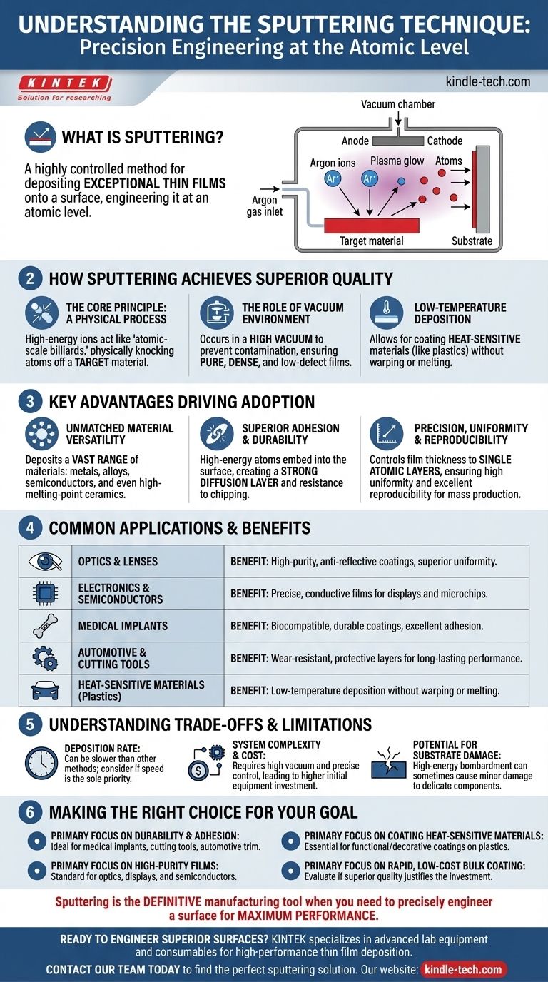
At its core, the sputtering technique is a highly controlled method for depositing exceptionally thin films of material onto a surface. This process is widely used across industries to enhance or alter the properties of a product, with common applications ranging from anti-reflective coatings on optical lenses and protective layers on automotive parts to conductive films in consumer electronics and biocompatible coatings on medical implants.
Sputtering is not just about coating a surface; it's about engineering that surface at an atomic level. Its primary value lies in its ability to deposit a vast range of materials with superior adhesion, purity, and uniformity, making it an indispensable tool for high-performance and high-precision manufacturing.
How Sputtering Achieves Superior Film Quality
To understand the applications of sputtering, you must first understand the physical process that gives it such unique advantages. It is fundamentally different from simple painting or dipping.
The Core Principle: A Physical Process
Sputtering is a physical vapor deposition (PVD) method. Imagine a high-energy particle, typically an ion, acting like a cue ball in a game of atomic-scale billiards.
This particle is accelerated in a vacuum chamber and strikes a block of the desired coating material, known as the target. The impact physically knocks atoms off the target's surface, "sputtering" them away with significant kinetic energy.
These ejected atoms then travel through the vacuum and deposit onto the component to be coated, called the substrate, forming a thin, dense, and uniform film.
The Role of the Vacuum Environment
The entire process occurs in a high vacuum to prevent the sputtered atoms from colliding with air or other contaminants.
This ensures the resulting film is exceptionally pure and dense, with far fewer defects or pinholes compared to other methods. This purity is critical for applications in optics and semiconductors.
Low-Temperature Deposition on Sensitive Materials
While the sputtered atoms themselves have high energy, the overall process does not significantly heat the substrate.
This is a key advantage, as it allows for the coating of heat-sensitive materials like plastics and other polymers without causing them to warp or melt.
The Key Advantages Driving Its Adoption
The specific characteristics of the sputtering process are what make it the preferred choice for so many demanding applications.
Unmatched Material Versatility
Virtually any substance can be used as a target material. This includes metals, alloys, semiconductors, and even insulating ceramics or compounds with extremely high melting points that are difficult or impossible to deposit using heat-based evaporation techniques.
Superior Adhesion and Durability
Because the sputtered atoms arrive at the substrate with high kinetic energy, they embed themselves slightly into the surface. This creates a strong diffusion layer and exceptional adhesion between the film and the substrate, resulting in a coating that is far more durable and resistant to chipping or flaking.
Precision, Uniformity, and Reproducibility
The thickness of the sputtered film can be controlled with extreme precision, often down to the level of single atomic layers. This is typically managed by adjusting the electrical current and the deposition time.
This control allows for highly uniform films over large areas and makes the process exceptionally reproducible, which is essential for mass production in industries like electronics and automotive manufacturing.
Understanding the Trade-offs and Limitations
No technique is perfect for every scenario. To make an informed decision, you must be aware of sputtering's potential downsides.
Deposition Rate
Generally, sputtering can be a slower deposition process compared to other methods like thermal evaporation. For applications where speed is the only priority and film quality is secondary, it may not be the most efficient choice.
System Complexity and Cost
Sputtering systems require a high vacuum, powerful electronics, and precisely controlled gas flow. This makes the initial equipment investment more significant than simpler coating methods.
Potential for Substrate Damage
The same high-energy particle bombardment that ensures great adhesion can, in some sensitive applications, cause minor structural damage to the substrate material. This is a critical consideration when developing processes for delicate electronic components.
Making the Right Choice for Your Goal
Sputtering is chosen when the performance and quality of the final film are paramount. Use the following guide to determine if it aligns with your objective.
- If your primary focus is Durability and Adhesion: Sputtering is the ideal choice for creating hard, wear-resistant, or biocompatible coatings for items like medical implants, cutting tools, and automotive trim.
- If your primary focus is High-Purity Optical or Electronic Films: The control, purity, and uniformity of sputtering make it the standard for anti-reflective coatings, optical filters, and conductive layers in displays and semiconductors.
- If your primary focus is Coating Heat-Sensitive Materials: Sputtering's low-temperature nature is essential for applying functional or decorative coatings onto plastics used in consumer goods, car headlights, and more.
- If your primary focus is Rapid, Low-Cost Bulk Coating: You should evaluate whether the superior quality of a sputtered film justifies the potentially slower deposition rate and higher equipment cost compared to other methods.
Ultimately, sputtering is the definitive manufacturing tool when you need to precisely engineer a surface for maximum performance.
Summary Table:
| Application Area | Key Benefit of Sputtering |
|---|---|
| Optics & Lenses | High-purity, anti-reflective coatings with superior uniformity |
| Electronics & Semiconductors | Precise, conductive films for displays and microchips |
| Medical Implants | Biocompatible, durable coatings with excellent adhesion |
| Automotive & Cutting Tools | Wear-resistant, protective layers for long-lasting performance |
| Heat-Sensitive Materials (e.g., Plastics) | Low-temperature deposition without warping or melting |
Ready to Engineer Superior Surfaces with Precision Sputtering?
At KINTEK, we specialize in providing advanced lab equipment and consumables for high-performance thin film deposition. Whether you're developing durable coatings for medical devices, high-purity optical films, or conductive layers for next-generation electronics, our sputtering solutions deliver the adhesion, uniformity, and material versatility your projects demand.
Let’s discuss how our expertise can enhance your manufacturing process. Contact our team today to find the perfect sputtering solution for your laboratory needs.
Visual Guide
Related Products
- RF PECVD System Radio Frequency Plasma-Enhanced Chemical Vapor Deposition RF PECVD
- Evaporation Boat for Organic Matter
- Chemical Vapor Deposition CVD Equipment System Chamber Slide PECVD Tube Furnace with Liquid Gasifier PECVD Machine
- Aluminized Ceramic Evaporation Boat for Thin Film Deposition
- Ceramic Evaporation Boat Set Alumina Crucible for Laboratory Use
People Also Ask
- What is the principle of plasma enhanced chemical vapor deposition? Achieve Low-Temperature Thin Film Deposition
- How are PECVD and CVD different? A Guide to Choosing the Right Thin-Film Deposition Process
- Why does PECVD commonly use RF power input? For Precise Low-Temperature Thin Film Deposition
- Why is PECVD environment friendly? Understanding the Eco-Friendly Benefits of Plasma-Enhanced Coating
- What are the advantages of PECVD? Enable Low-Temperature, High-Quality Thin-Film Deposition