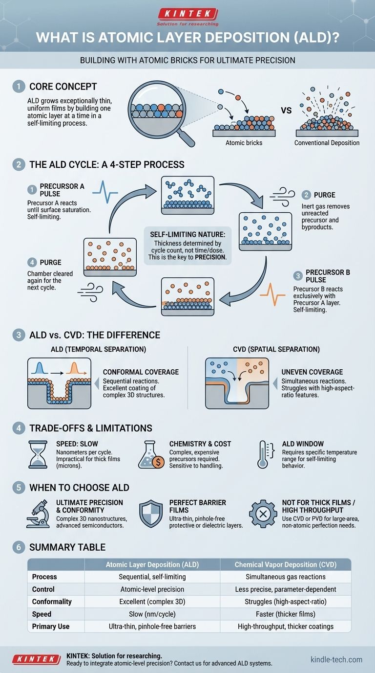
At its core, Atomic Layer Deposition (ALD) is a fabrication technique used to grow exceptionally thin and uniform films of material onto a substrate. It achieves this by exposing the surface to a sequence of different chemical gases, or precursors, one at a time. Each gas pulse forms exactly one atomic layer (or a fraction of a layer) in a self-limiting reaction, allowing for the construction of a film with atomic-level precision.
Unlike conventional deposition methods that continuously "spray" material onto a surface, ALD functions like building with individual atomic bricks. This sequential, self-completing process grants unparalleled control over film thickness and the ability to perfectly coat highly complex 3D surfaces.
How an ALD Cycle Works: A Step-by-Step Process
Understanding ALD requires understanding its fundamental cycle, which is repeated to build up the film to the desired thickness. The process is defined by its separation of precursor reactions in time.
Step 1: Precursor A Pulse and Purge
First, a pulse of the first precursor gas (Precursor A) is introduced into the reaction chamber. The gas molecules react with the substrate's surface until all available reactive sites are occupied.
Once the surface is saturated, the reaction stops on its own. Any excess, unreacted gas and reaction byproducts are then purged from the chamber with an inert gas like nitrogen or argon.
Step 2: Precursor B Pulse and Purge
Next, a pulse of the second precursor gas (Precursor B) is introduced. This precursor reacts exclusively with the layer of Precursor A that was just deposited, not with the underlying substrate.
This second reaction is also self-limiting. Once all the sites on the new surface layer are occupied, the reaction ceases. The chamber is then purged again to remove any excess gas and byproducts.
The Self-Limiting Nature: The Key to Precision
This two-step cycle constitutes the deposition of a single layer of the final material. Because each step only proceeds until the surface is fully saturated, the amount of material deposited per cycle is constant and predictable.
This self-limiting behavior is the defining characteristic of ALD. It means the final film thickness is determined simply by the number of cycles performed, not by the precise dose of the precursor or the timing of the pulse. This is the source of ALD's legendary precision.
ALD vs. Chemical Vapor Deposition (CVD): The Critical Difference
To appreciate ALD's unique value, it is essential to compare it to a more common technique like Chemical Vapor Deposition (CVD).
Spacial vs. Temporal Separation
In CVD, all precursor gases are present in the chamber at the same time, reacting simultaneously in the gas phase and on the substrate surface. The reactions are separated spatially.
In ALD, the precursors are separated temporally—introduced one after another. This prevents gas-phase reactions and ensures growth only happens on the surface, layer by layer.
Conformal Coverage
Because ALD reactions are self-limiting, they can penetrate and perfectly coat extremely complex, high-aspect-ratio structures like deep trenches and pores. The film will have the same thickness everywhere, from the top surface to the very bottom of a microscopic hole. This is called conformal coverage.
CVD often struggles with this, leading to thicker deposits at the entrance of a feature and thinner, incomplete coverage inside.
Understanding the Trade-offs
Despite its advantages, ALD is not a universal solution. Its unique mechanism comes with inherent limitations that must be considered.
The Primary Limitation: Speed
ALD is an inherently slow process. Since each cycle deposits only a fraction of a nanometer of material, building up a film of even tens of nanometers can take a significant amount of time.
This makes ALD impractical for applications requiring thick films (microns or more), where techniques like CVD or PVD are far more efficient.
Precursor Chemistry and Cost
Developing a successful ALD process requires finding a pair of precursor chemicals that have ideal, self-limiting reactivity within a specific temperature range. These precursors can be complex, expensive, and sensitive to handling.
The "ALD Window"
The self-limiting behavior only occurs within a specific range of temperatures known as the "ALD window." Below this temperature, reactions may be too slow or incomplete. Above it, the precursor chemicals might decompose on their own, leading to uncontrolled, CVD-like growth that negates the benefits of ALD.
Making the Right Choice for Your Application
Selecting the right deposition technique requires aligning the method's strengths with your primary engineering goal.
- If your primary focus is ultimate precision and conformity: ALD is the superior choice for coating complex 3D nanostructures or when exact atomic-level thickness is non-negotiable, as in advanced semiconductor gates.
- If your primary focus is high throughput for thick films: A technique like Chemical Vapor Deposition (CVD) or Physical Vapor Deposition (PVD) is far more practical for large-area coatings where atomic perfection is not the main driver.
- If your primary focus is creating a perfect, pinhole-free barrier: ALD's layer-by-layer growth is ideal for creating ultra-thin protective or dielectric films that must be flawless to prevent diffusion or electrical leakage.
Ultimately, understanding the principle of self-limiting reactions is the key to deciding when ALD's precision justifies its deliberate pace.
Summary Table:
| Feature | Atomic Layer Deposition (ALD) | Chemical Vapor Deposition (CVD) |
|---|---|---|
| Process | Sequential, self-limiting reactions | Simultaneous gas reactions |
| Control | Atomic-level precision | Less precise, depends on parameters |
| Conformality | Excellent for complex 3D structures | Struggles with high-aspect-ratio features |
| Speed | Slow (nanometers per cycle) | Faster (suitable for thicker films) |
| Primary Use | Ultra-thin, pinhole-free barriers | High-throughput, thicker coatings |
Ready to integrate atomic-level precision into your lab workflows? At KINTEK, we specialize in providing advanced lab equipment, including ALD systems, to help you achieve flawless thin films and coatings for your most demanding applications. Whether you're in semiconductor research, nanotechnology, or materials science, our solutions are designed to meet your precision needs. Contact our experts today to discuss how ALD can transform your research and development.
Visual Guide
Related Products
- RF PECVD System Radio Frequency Plasma-Enhanced Chemical Vapor Deposition RF PECVD
- Chemical Vapor Deposition CVD Equipment System Chamber Slide PECVD Tube Furnace with Liquid Gasifier PECVD Machine
- Aluminized Ceramic Evaporation Boat for Thin Film Deposition
- HFCVD Machine System Equipment for Drawing Die Nano-Diamond Coating
- 915MHz MPCVD Diamond Machine Microwave Plasma Chemical Vapor Deposition System Reactor
People Also Ask
- What is an example of PECVD? RF-PECVD for High-Quality Thin Film Deposition
- What is the role of RF-PECVD in VFG preparation? Mastering Vertical Growth and Surface Functionality
- What is plasma enhanced chemical vapour deposition process? Unlock Low-Temperature, High-Quality Thin Films
- Why is a Matching Network Indispensable in RF-PECVD for Siloxane Films? Ensure Stable Plasma and Uniform Deposition
- What is plasma CVD? Unlock Low-Temperature Thin Film Deposition for Sensitive Materials


