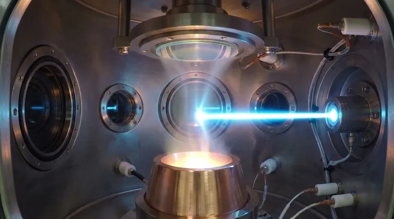
In short, beam deposition is a sophisticated process that uses a focused, high-energy beam of electrons or ions inside a vacuum to turn a solid source material into a vapor. This vapor then travels and condenses onto a target object, forming an extremely thin, pure, and precisely controlled coating or film.
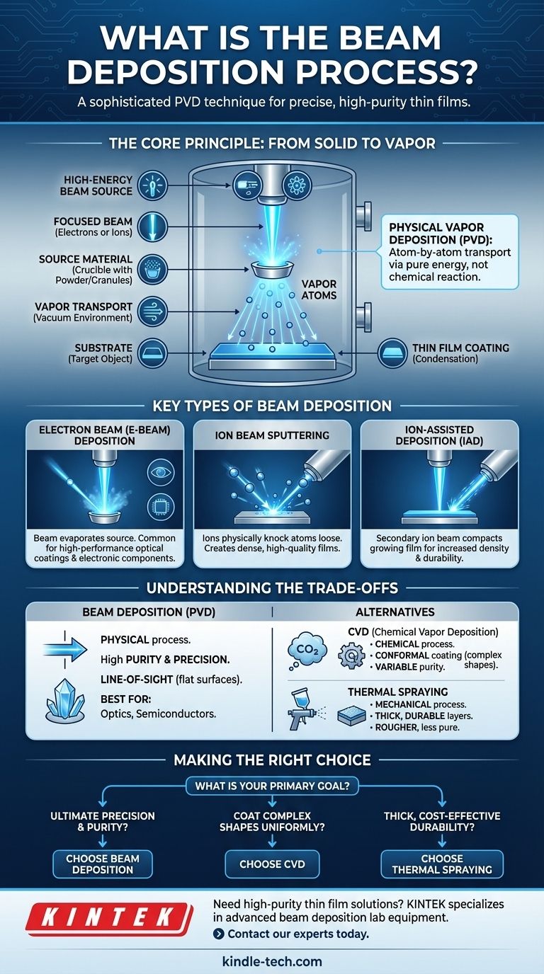
Beam deposition is fundamentally a Physical Vapor Deposition (PVD) technique prized for its precision. Unlike chemical methods, it uses pure energy—not a chemical reaction—to transport material atom-by-atom, resulting in high-quality films essential for optics, electronics, and advanced materials.
The Core Principle: From Solid to Vapor
The Role of the High-Energy Beam
The defining feature of this process is the use of a focused beam as an energy source. This beam, typically composed of either electrons or ions, is aimed at a target material (often in the form of powder or granules) held in a crucible.
The intense energy from the beam heats the source material to its boiling point, causing it to vaporize.
The Vacuum Environment
The entire process occurs within a high-vacuum chamber. This is critical for two reasons: it prevents the vaporized material from reacting with air, ensuring the purity of the final film, and it allows the vapor atoms to travel in a straight line from the source to the substrate without colliding with other particles.
Condensation and Film Growth
Once the vaporized atoms reach the cooler surface of the object being coated (the substrate), they condense back into a solid state. This happens layer by layer, forming a thin, uniform film.
Through precise computer control of the beam's power, vacuum level, and substrate positioning, the thickness and properties of the coating can be managed with exceptional accuracy.
Key Types of Beam Deposition
Electron Beam (E-Beam) Deposition
This is the most common form of beam deposition. A high-energy electron beam is magnetically guided to strike the source material, causing it to evaporate. E-beam deposition is widely used for creating high-performance optical coatings and electronic components.
Ion Beam Sputtering
Sputtering uses a slightly different mechanism. Instead of vaporizing the material with heat, a high-energy ion beam bombards a solid target. The force of the ion impacts is enough to physically knock atoms loose from the target—a process called "sputtering."
These ejected atoms then travel through the vacuum and deposit onto the substrate.
Ion-Assisted Deposition (IAD)
This is not a standalone method but an enhancement to another process, like E-beam deposition. While the film is being deposited, a second, low-energy ion beam is aimed at the substrate.
This ionic bombardment compacts the growing film, increasing its density, durability, and adhesion to the substrate. The result is a more robust and stable coating.
Understanding the Trade-offs: Beam Deposition vs. Other Methods
Comparison with Chemical Vapor Deposition (CVD)
CVD is a chemical process, not a physical one. In CVD, the part is placed in a chamber filled with reactive gases. A chemical reaction occurs on the hot surface of the part, leaving behind a solid film.
Unlike the line-of-sight nature of beam deposition, the gases in CVD can coat complex shapes and internal surfaces more easily. However, the process is limited by the available chemical reactions and can introduce impurities.
Comparison with Thermal Spraying
Spraying is a more mechanical process where droplets or particles of molten or semi-molten material are sprayed onto a surface. It is excellent for applying thick, protective coatings but lacks the atomic-level precision of beam deposition.
The films produced by spraying are generally much thicker, rougher, and less pure than those from beam deposition.
Key Advantages of Beam Deposition
The primary benefits are purity and control. Because it operates in a high vacuum and vaporizes pure source material, the resulting films are exceptionally clean. The use of a focused beam allows for precise control over the deposition rate and film thickness.
Potential Limitations
Beam deposition is a line-of-sight process. The vapor travels in a straight line, which can make it difficult to uniformly coat objects with complex, three-dimensional shapes. The equipment required is also highly specialized and can be more expensive than simpler methods.
Making the Right Choice for Your Goal
Selecting the correct deposition method depends entirely on the desired outcome for the final product.
- If your primary focus is ultimate precision and purity (e.g., optical filters, semiconductors): Beam deposition is the superior choice for its unmatched control over film thickness and material purity.
- If your primary focus is coating complex shapes uniformly (e.g., internal pipes, machine parts): Chemical Vapor Deposition (CVD) is often more suitable because the precursor gases can flow around and into intricate geometries.
- If your primary focus is creating thick, durable coatings cost-effectively (e.g., corrosion resistance): Thermal spraying provides a robust and economical solution when atomic-level precision is not required.
Ultimately, understanding the fundamental difference between physical transport (beam deposition) and chemical reaction (CVD) is the key to selecting the right tool for your engineering challenge.
Summary Table:
| Feature | Beam Deposition (PVD) | Chemical Vapor Deposition (CVD) | Thermal Spraying |
|---|---|---|---|
| Process Type | Physical (Energy) | Chemical (Reaction) | Mechanical (Spray) |
| Coating Thickness | Very Thin, Precise | Thin to Moderate | Thick |
| Coating Uniformity | Line-of-Sight | Excellent for Complex Shapes | Variable |
| Primary Advantage | High Purity & Precision | Conformal Coating | Thick, Durable Layers |
| Best For | Optics, Semiconductors | Complex 3D Parts | Corrosion Resistance |
Need a high-purity thin film for your application?
KINTEK specializes in advanced lab equipment, including beam deposition systems, to help you achieve the ultimate in coating precision and purity. Our expertise ensures you get the right solution for your specific needs in optics, electronics, or materials research.
Contact our experts today to discuss how our solutions can enhance your laboratory's capabilities.
Visual Guide
Related Products
- Electron Beam Evaporation Coating Oxygen-Free Copper Crucible and Evaporation Boat
- RF PECVD System Radio Frequency Plasma-Enhanced Chemical Vapor Deposition RF PECVD
- Chemical Vapor Deposition CVD Equipment System Chamber Slide PECVD Tube Furnace with Liquid Gasifier PECVD Machine
- HFCVD Machine System Equipment for Drawing Die Nano-Diamond Coating
- Inclined Rotary Plasma Enhanced Chemical Vapor Deposition PECVD Equipment Tube Furnace Machine
People Also Ask
- What are the applications of e-beam evaporation? Achieve High-Purity Coatings for Optics & Electronics
- What is e-beam evaporation? Achieve High-Purity Thin Film Deposition for Your Lab
- What is the temperature of e-beam evaporation? Mastering the Two-Zone Thermal Process for Precision Films
- What is e-beam evaporation used for? Precision Coating for Optics, Aerospace & Electronics
- What are the applications of electron beams? From Nanoscale Imaging to Industrial Manufacturing


