At its core, e-beam evaporation is a highly current and versatile physical vapor deposition (PVD) method for creating high-purity thin films. The process uses a magnetically focused beam of high-energy electrons to vaporize materials, which then condense onto a substrate. It remains a critical technology in demanding fields like electronics, aerospace, and optics, especially for materials with very high melting points.
Electron beam evaporation is the go-to solution when you need to deposit exceptionally pure films from a wide variety of materials, including metals and ceramics that are difficult to process with other methods. Its primary strengths are high deposition rates and material versatility, traded against moderate system complexity.
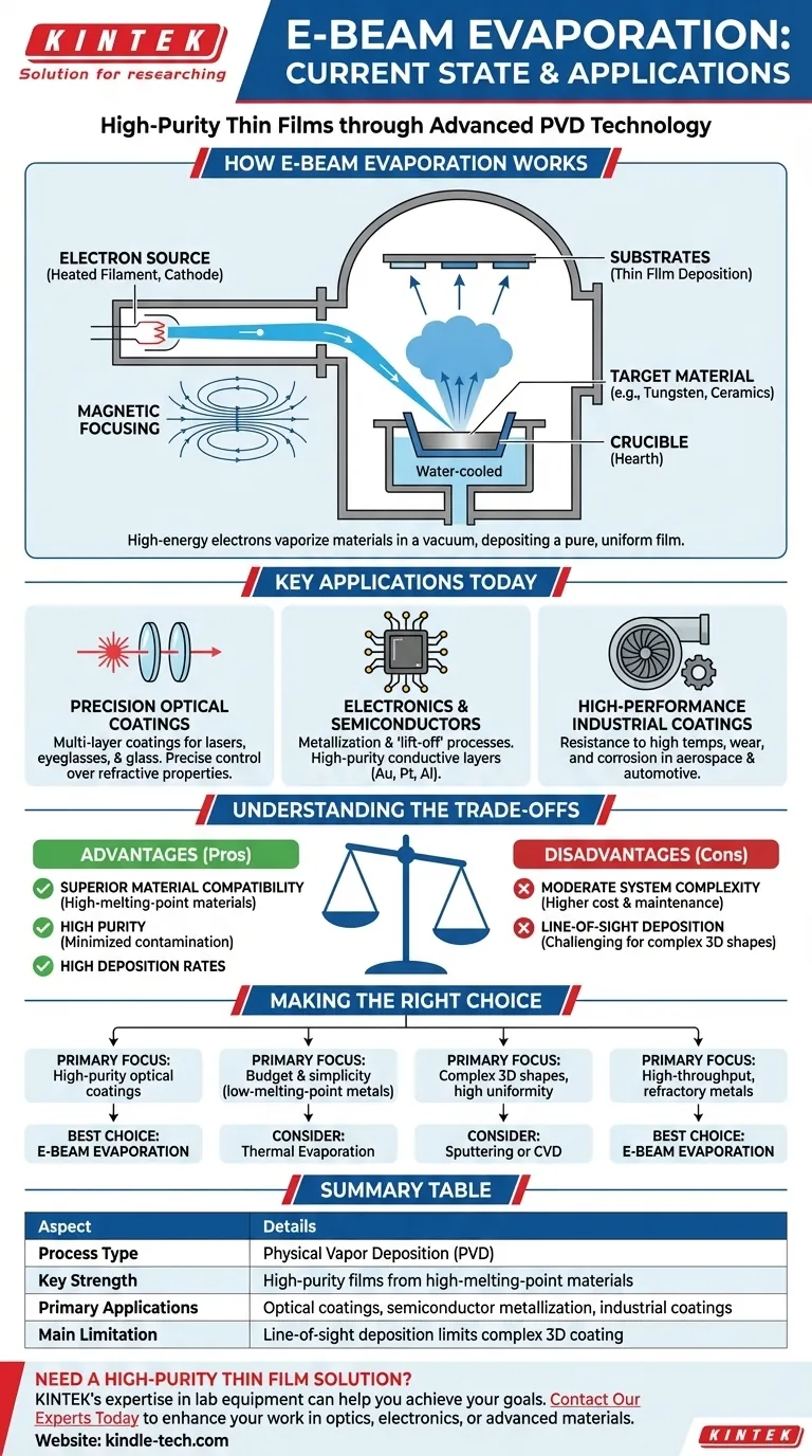
How E-Beam Evaporation Works: The Core Principle
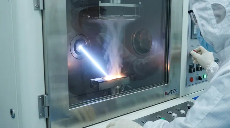
To understand its modern applications, we must first understand the process itself. It is a refined technique that takes place within a high-vacuum chamber.
The Electron Source
A heated filament, or cathode, releases a high-energy stream of electrons. These electrons are then accelerated toward the target material using a very high voltage.
Magnetic Focusing
Powerful magnetic fields are used to precisely bend and focus this stream of electrons. This allows for immense energy to be concentrated onto a very small spot within a crucible.
Vaporization and Deposition
The target material, held in a water-cooled copper hearth or crucible, is heated by the electron beam to its vaporization point. This vapor then travels in a straight line, depositing as a thin, uniform film on the substrates positioned above it.
Where E-Beam Evaporation Is Used Today
E-beam evaporation is not a niche or outdated technology; it is a workhorse in several advanced industries where film quality is paramount.
Precision Optical Coatings
The process is ideal for creating multi-layer coatings for laser optics, eyeglasses, and architectural glass. Its ability to deposit high-purity dielectric materials like silicon dioxide allows for precise control over refractive properties.
Electronics and Semiconductors
In electronics manufacturing, e-beam is used for metallization and "lift-off" processes. It can deposit conductive layers of materials like gold, platinum, or aluminum with high purity, which is critical for device performance.
High-Performance Industrial Coatings
Industries from aerospace to automotive rely on e-beam evaporation to apply coatings that provide resistance to high temperatures, wear, and chemical corrosion.
Understanding the Trade-offs
No single technology is perfect for every scenario. Choosing e-beam evaporation requires understanding its distinct advantages and limitations compared to other methods like sputtering or chemical vapor deposition (CVD).
Advantage: Superior Material Compatibility
This is arguably the greatest strength of e-beam evaporation. It can deposit materials with extremely high melting points, such as tungsten and tantalum, that are impossible to process using simpler thermal evaporation techniques.
Advantage: High Purity and Deposition Rates
Because only the target material is heated directly by the electron beam, contamination from the crucible is minimized, resulting in very pure films. The deposition rates are also typically higher than those achieved with sputtering.
Disadvantage: Moderate System Complexity
The use of high-voltage electron guns and magnetic focusing systems makes e-beam systems more complex and costly than basic thermal evaporators.
Disadvantage: Line-of-Sight Deposition
Like most PVD techniques, e-beam is a "line-of-sight" process. This means it can be challenging to coat complex, three-dimensional shapes uniformly, an area where methods like CVD can have an advantage.
Making the Right Choice for Your Application
Selecting the correct deposition method depends entirely on your project's specific goals for material, purity, and geometry.
- If your primary focus is high-purity optical coatings: E-beam evaporation is an ideal choice due to its precise control and compatibility with a vast range of dielectric materials.
- If your primary focus is budget and simplicity for low-melting-point metals: A simpler thermal evaporation system may be a more cost-effective solution.
- If your primary focus is coating complex 3D shapes with high uniformity: You should evaluate sputtering or chemical vapor deposition (CVD) as potential alternatives.
- If your primary focus is high-throughput deposition of refractory metals: E-beam's high deposition rates and material compatibility give it a significant advantage.
Ultimately, e-beam evaporation remains a vital and current technology for any application demanding high-purity thin films from a diverse palette of materials.
Summary Table:
| Aspect | Details |
|---|---|
| Process Type | Physical Vapor Deposition (PVD) |
| Key Strength | High-purity films from high-melting-point materials |
| Primary Applications | Optical coatings, semiconductor metallization, industrial coatings |
| Main Limitation | Line-of-sight deposition limits coating of complex 3D shapes |
Need a high-purity thin film deposition solution for your lab?
E-beam evaporation is a powerful technique for depositing high-purity films from a wide range of materials, including refractory metals and ceramics. If your research or production demands exceptional film quality and material versatility, KINTEK's expertise in lab equipment can help you achieve your goals.
We specialize in providing reliable solutions for laboratory needs. Contact our experts today to discuss how our e-beam evaporation systems can enhance your work in optics, electronics, or advanced materials development.
Visual Guide
Related Products
- Electron Beam Evaporation Coating Oxygen-Free Copper Crucible and Evaporation Boat
- Electron Beam Evaporation Coating Tungsten Crucible and Molybdenum Crucible for High Temperature Applications
- Electron Beam Evaporation Coating Gold Plating Tungsten Molybdenum Crucible for Evaporation
- Electron Beam Evaporation Coating Conductive Boron Nitride Crucible BN Crucible
- E Beam Crucibles Electron Gun Beam Crucible for Evaporation
People Also Ask
- What is the container that holds the metal source material called in e-beam evaporation? Ensure Purity and Quality in Your Thin-Film Deposition
- What is e-beam evaporation used for? Precision Coating for Optics, Aerospace & Electronics
- What are the applications of e-beam evaporation? Achieve High-Purity Coatings for Optics & Electronics
- What is e-beam evaporation? Achieve High-Purity Thin Film Deposition for Your Lab
- What is the temperature of e-beam evaporation? Mastering the Two-Zone Thermal Process for Precision Films


