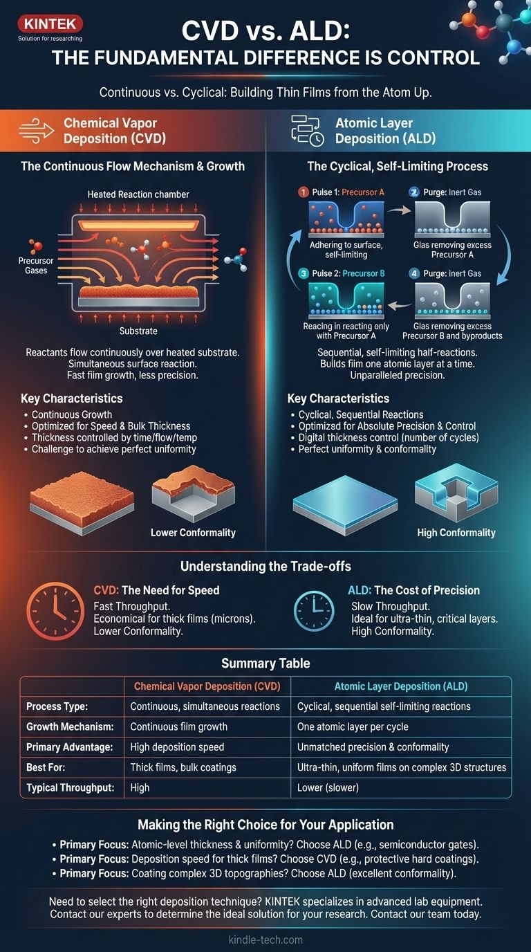
In short, the fundamental difference between Chemical Vapor Deposition (CVD) and Atomic Layer Deposition (ALD) is control. CVD is a continuous process where precursor gases react simultaneously on a substrate surface, making it fast but less precise. ALD is a cyclical, sequential process where gases are introduced one at a time, creating a self-limiting reaction that allows for the deposition of a single, perfect atomic layer per cycle, offering unparalleled precision.
While both methods build thin films from chemical gases, the core distinction is their growth mechanism. CVD is a continuous process optimized for speed and bulk thickness, while ALD is a sequential, self-limiting process optimized for absolute precision, uniformity, and control at the atomic scale.
Understanding the Chemical Vapor Deposition (CVD) Process
The Continuous Flow Mechanism
In a CVD process, one or more reactive precursor gases are continuously introduced into a reaction chamber. These gases flow over a heated substrate.
Surface Reaction and Growth
The heat provides the necessary thermal energy for the precursor gases to react or decompose on the substrate's surface. This chemical reaction forms a stable, solid thin film.
Key Characteristics of CVD
Film growth is continuous as long as the gases are flowing and the temperature is maintained. Thickness is controlled by managing the deposition time, gas flow rates, and temperature. This method is relatively fast, but achieving perfect uniformity can be a challenge.
The Atomic Layer Deposition (ALD) Revolution
A Cyclical, Self-Limiting Process
ALD refines the CVD concept by breaking the continuous reaction into two distinct, self-limiting half-reactions. A complete ALD cycle consists of four sequential steps that are repeated to build the film layer by atomic layer.
Step 1: First Precursor Pulse
The first precursor gas (A) is pulsed into the chamber. It reacts with the substrate surface until every available reaction site is occupied. This reaction is self-limiting; once the surface is saturated, no more precursor can attach.
Step 2: Purge
An inert gas, like nitrogen or argon, is used to purge the chamber. This step completely removes any excess, unreacted precursor A molecules.
Step 3: Second Precursor Pulse
The second precursor gas (B) is pulsed into the chamber. It reacts exclusively with the layer of precursor A that is already chemically bonded to the surface. This reaction is also self-limiting.
Step 4: Purge
The chamber is purged again with the inert gas to remove any unreacted precursor B and the byproducts from the reaction. At the end of this step, exactly one monolayer of the final material has been deposited.
The Result: Unmatched Precision
The film's final thickness is determined simply by the number of ALD cycles performed. This gives engineers digital, sub-nanometer control over the final product, which is impossible to achieve with conventional CVD.
Understanding the Trade-offs
The Cost of Precision
ALD’s greatest strength—its precision—is also linked to its primary weakness: speed. Building a film one atomic layer at a time is inherently slow. The throughput of ALD is significantly lower than that of CVD, making it less economical for applications requiring thick films (in the micron range).
Conformality vs. Speed
The self-limiting nature of ALD allows it to perfectly coat extremely complex, three-dimensional structures with a uniform film. This is known as high conformality. CVD struggles with such structures, often resulting in thicker deposits at the opening of a feature and thinner deposits at the bottom.
Process Temperature and Material Quality
Because ALD reactions are so controlled, they can often be performed at lower temperatures than CVD. This makes ALD suitable for temperature-sensitive substrates. The purge steps also ensure extremely high-purity films with fewer defects and higher density.
Making the Right Choice for Your Application
Selecting the correct deposition technique requires a clear understanding of your project's primary goal.
- If your primary focus is atomic-level thickness control and perfect uniformity: Choose ALD for critical applications like semiconductor gate oxides, barrier layers in integrated circuits, or coating complex nanoscale structures.
- If your primary focus is deposition speed for thicker films: Choose CVD for applications like thick protective hard coatings on machine tools, optical films, or bulk semiconductor layers where minor variations in thickness are acceptable.
- If your primary focus is coating complex 3D topographies with high fidelity: ALD is the superior choice due to its excellent conformality, ensuring every surface is coated evenly.
Ultimately, understanding this fundamental difference between continuous (CVD) and cyclical (ALD) growth empowers you to select the precise tool needed to build materials from the atom up.
Summary Table:
| Feature | Chemical Vapor Deposition (CVD) | Atomic Layer Deposition (ALD) |
|---|---|---|
| Process Type | Continuous, simultaneous reactions | Cyclical, sequential self-limiting reactions |
| Growth Mechanism | Continuous film growth | One atomic layer per cycle |
| Primary Advantage | High deposition speed | Unmatched precision & conformality |
| Best For | Thick films, bulk coatings | Ultra-thin, uniform films on complex 3D structures |
| Typical Throughput | High | Lower (slower) |
Need to select the right deposition technique for your specific materials or application? The choice between CVD and ALD is critical for achieving optimal film quality, uniformity, and performance. KINTEK specializes in providing advanced lab equipment and consumables for precise thin-film deposition. Our experts can help you determine the ideal solution—whether you prioritize the speed of CVD or the atomic-level control of ALD—to enhance your research and development outcomes. Contact our team today to discuss your laboratory's unique needs and discover how our solutions can drive your success.
Visual Guide
Related Products
- Chemical Vapor Deposition CVD Equipment System Chamber Slide PECVD Tube Furnace with Liquid Gasifier PECVD Machine
- RF PECVD System Radio Frequency Plasma-Enhanced Chemical Vapor Deposition RF PECVD
- Microwave Plasma Chemical Vapor Deposition MPCVD Machine System Reactor for Lab and Diamond Growth
- Customer Made Versatile CVD Tube Furnace Chemical Vapor Deposition Chamber System Equipment
- 915MHz MPCVD Diamond Machine Microwave Plasma Chemical Vapor Deposition System Reactor
People Also Ask
- What are the processes of vapor phase deposition? Understand CVD vs. PVD for Superior Thin Films
- What is the chemical vapor deposition growth process? Build Superior Thin Films from the Atom Up
- What are the core advantages of PE-CVD in OLED encapsulation? Protect Sensitive Layers with Low-Temp Film Deposition
- What are the advantages of chemical vapor deposition? Achieve Superior Thin Films for Your Lab
- What is plasma enhanced chemical vapor deposition PECVD equipment? A Guide to Low-Temperature Thin Film Deposition


