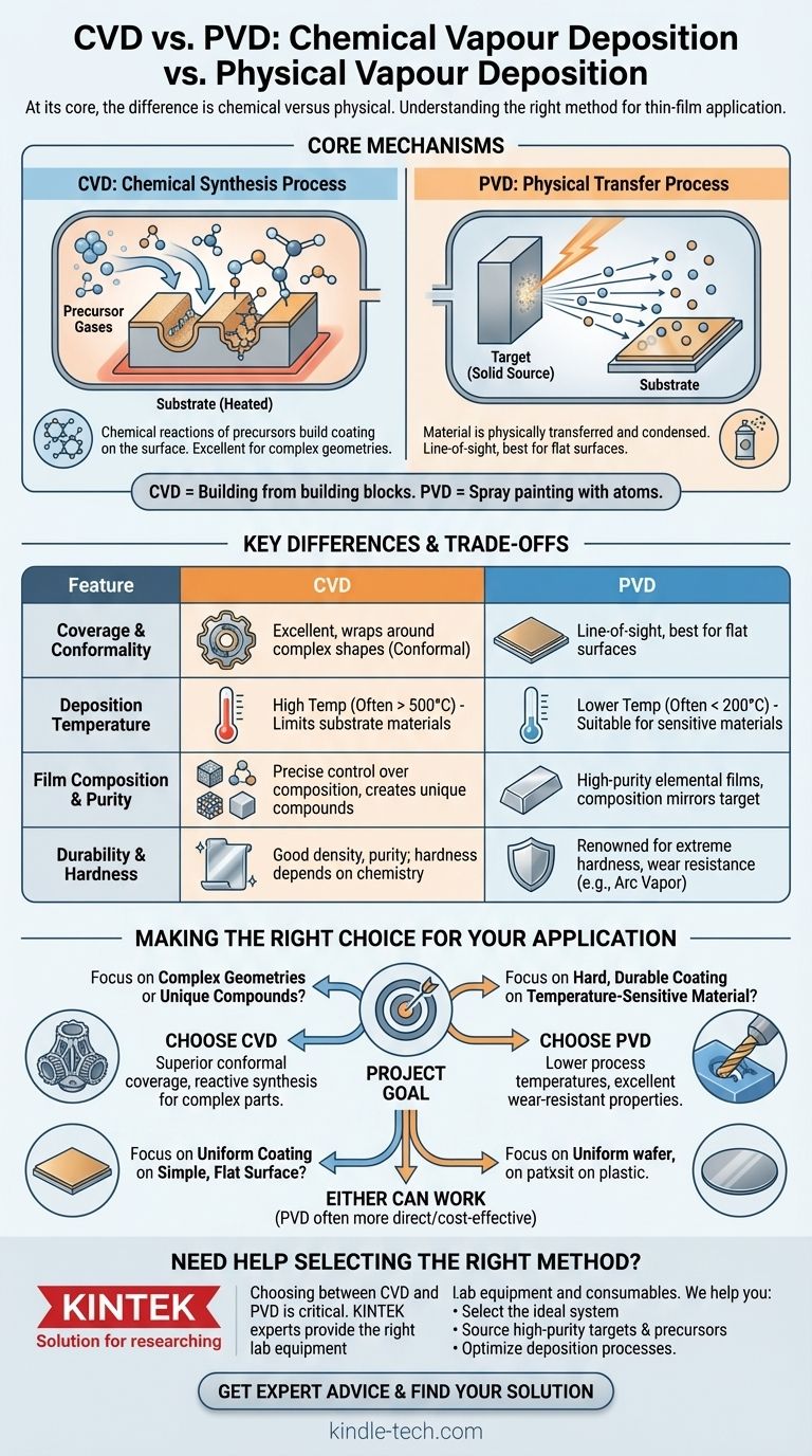
At its core, the difference is chemical versus physical. Chemical Vapor Deposition (CVD) uses chemical reactions between precursor gases on a heated surface to create a new material as a solid film. In contrast, Physical Vapor Deposition (PVD) physically transfers a material from a solid source to a substrate, vaporizing it in a vacuum and allowing it to condense as a thin film without a chemical change.
The essential distinction is this: CVD is a synthesis process that builds a coating from chemical building blocks on the substrate's surface. PVD is a transfer process that moves an existing material from a source to the substrate, like spray painting with atoms.
Understanding the Core Mechanisms
To choose the right method, you must first understand their fundamentally different approaches to building a thin film. One is based on chemistry, the other on physics.
Physical Vapor Deposition (PVD): A Line-of-Sight Transfer
PVD takes place within a high-vacuum chamber. A solid source material, known as the target, is vaporized through physical means.
These vaporized atoms or molecules travel in a straight line through the vacuum and condense onto the substrate, forming the coating.
Because the atoms travel in a direct path, PVD is considered a line-of-sight process. This is highly effective for coating flat surfaces but can struggle with complex, three-dimensional shapes.
Chemical Vapor Deposition (CVD): A Surface-Based Reaction
In a CVD process, one or more volatile precursor gases are introduced into a reaction chamber.
These gases are not the coating material itself, but the chemical ingredients. When they come into contact with a heated substrate, they react or decompose on the surface, forming a solid film of a new material.
Because the process is governed by the flow of gas and surface chemistry, CVD can deposit highly conformal coatings that perfectly wrap around complex shapes and even coat internal surfaces.
How the Process Affects Coating Properties
The differences in mechanism directly lead to different coating characteristics. The choice between PVD and CVD often comes down to which of these properties is most critical for your application.
Coverage and Conformality
CVD's use of gas precursors allows it to achieve excellent wrap-around properties. The gas can reach every exposed surface of a part, making it ideal for coating complex components.
PVD’s line-of-sight nature means it excels at coating surfaces directly facing the source. However, it struggles to uniformly coat undercuts, sharp corners, or the inside of tubes without complex fixtures and part rotation.
Deposition Temperature
CVD typically requires high temperatures (often several hundred to over 1000°C) to drive the necessary chemical reactions on the substrate's surface. This limits the types of materials that can be coated without being damaged.
PVD processes can often be performed at much lower temperatures (sometimes below 200°C). This makes PVD suitable for coating temperature-sensitive materials like plastics, aluminum alloys, or previously heat-treated steels.
Film Composition and Purity
CVD allows for precise control over the film's chemical composition, crystal structure, and morphology by adjusting the mixture and flow of precursor gases. It can be used to create a wide variety of materials, including metals, ceramics, and complex multi-component alloys.
PVD physically transfers the source material, so the coating's composition is largely identical to the target. This is excellent for depositing high-purity elemental films, and some variants allow for the blending of materials.
Durability and Hardness
PVD methods, particularly those involving ionization like Arc Vapor Deposition, are renowned for creating extremely hard, dense, and durable coatings. These films offer excellent resistance to wear and corrosion.
CVD films also exhibit good density and high purity. The stress within the film can often be lower than in PVD films, but specific hardness is highly dependent on the exact chemistry being deposited.
Understanding the Trade-offs
Neither method is universally superior. The optimal choice is a matter of balancing competing requirements.
The Temperature vs. Substrate Dilemma
The primary trade-off is often temperature. If your substrate cannot withstand the high heat of a traditional CVD process, PVD is the default choice. Specialized methods like Plasma-Enhanced CVD (PECVD) were developed specifically to lower CVD's temperature requirements.
The Complexity vs. Coverage Challenge
If you need to coat a complex part with uniform thickness, such as the inside of a mold or a porous structure, CVD is the far better option. For simpler geometries where a durable, hard surface is key, PVD's line-of-sight deposition is often more efficient and cost-effective.
Precursor Handling and Safety
A practical consideration is the nature of the source materials. PVD uses solid targets that are generally stable and safe to handle. CVD often relies on precursor gases that can be highly toxic, flammable, or corrosive, necessitating significant safety infrastructure.
Making the Right Choice for Your Application
Your final decision must be aligned with the most important outcome for your project.
- If your primary focus is coating complex internal geometries or creating unique compound films: Choose CVD for its superior conformal coverage and reactive synthesis capability.
- If your primary focus is applying a hard, durable coating to a temperature-sensitive material: Choose PVD for its lower process temperatures and excellent wear-resistant properties.
- If your primary focus is achieving a uniform coating on a simple, flat surface: Either method can work, but PVD is often a more direct and cost-effective solution.
Understanding the fundamental difference between chemical synthesis and physical transfer empowers you to select the right tool for your engineering goal.
Summary Table:
| Feature | Chemical Vapor Deposition (CVD) | Physical Vapor Deposition (PVD) |
|---|---|---|
| Core Mechanism | Chemical reaction of gases on a heated surface | Physical transfer of material in a vacuum |
| Coating Conformality | Excellent, wraps around complex shapes | Line-of-sight, best for flat surfaces |
| Typical Temperature | High (often > 500°C) | Low (can be < 200°C) |
| Ideal For | Complex geometries, unique compound films | Temperature-sensitive substrates, hard, durable coatings |
Need Help Selecting the Right Deposition Method for Your Project?
Choosing between CVD and PVD is critical for achieving the desired coating properties on your substrates. The experts at KINTEK specialize in providing the right lab equipment and consumables for your specific thin-film deposition needs.
We can help you:
- Select the ideal system based on your substrate material, desired film properties, and part geometry.
- Source high-purity targets and precursor gases to ensure consistent, high-quality results.
- Optimize your deposition process for maximum efficiency and performance.
Don't let the complexity of thin-film technologies slow down your research or production. Contact our technical team today for a personalized consultation and discover how KINTEK's solutions can advance your laboratory work.
Get Expert Advice & Find Your Solution
Visual Guide
Related Products
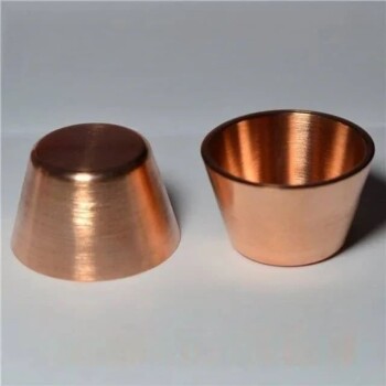
- Electron Beam Evaporation Coating Oxygen-Free Copper Crucible and Evaporation Boat
- Custom CVD Diamond Coating for Lab Applications
- Aluminized Ceramic Evaporation Boat for Thin Film Deposition
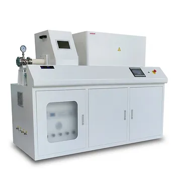
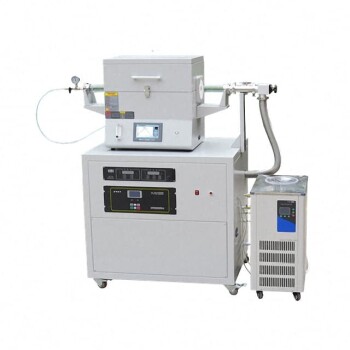
- Chemical Vapor Deposition CVD Equipment System Chamber Slide PECVD Tube Furnace with Liquid Gasifier PECVD Machine
- Customer Made Versatile CVD Tube Furnace Chemical Vapor Deposition Chamber System Equipment
People Also Ask
- What are the applications of e-beam evaporation? Achieve High-Purity Coatings for Optics & Electronics
- What is the deposition rate of e-beam evaporation? Control Thin Film Quality and Speed
- What is e-beam evaporation? Achieve High-Purity Thin Film Deposition for Your Lab
- What is the temperature of e-beam evaporation? Mastering the Two-Zone Thermal Process for Precision Films
- What is the voltage of e-beam evaporation? Achieve Precise Thin-Film Deposition
