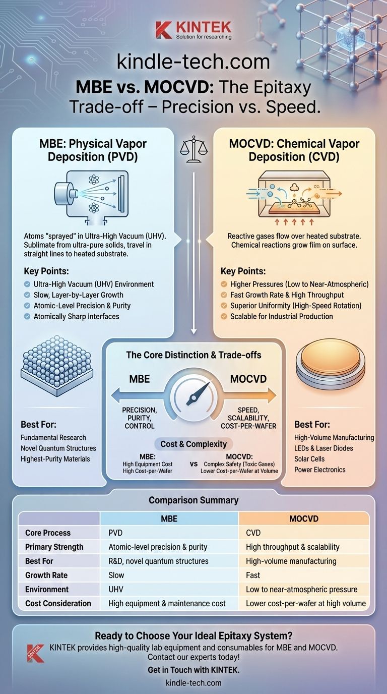
At its core, the difference between Molecular Beam Epitaxy (MBE) and Metalorganic Chemical Vapor Deposition (MOCVD) lies in how they deliver material to a substrate. MBE is a physical process that "sprays" atoms in a high vacuum, while MOCVD is a chemical process that uses reactive gases to "grow" a film on a surface. This fundamental distinction dictates their respective strengths: MBE offers unparalleled precision, while MOCVD delivers superior speed and scalability.
While both techniques produce high-quality crystalline thin films (epitaxy), the choice between them is a classic engineering trade-off. MBE is the tool of choice for ultimate purity and atomic-level control, whereas MOCVD is the workhorse for high-volume industrial production.
The Core Distinction: Physical vs. Chemical Deposition
The names of these techniques reveal their fundamental nature. One is based on a physical process (evaporation), while the other relies on chemical reactions.
MBE: A Physical Deposition Process
Molecular Beam Epitaxy is a refined form of Physical Vapor Deposition (PVD).
It works by heating ultra-pure solid elemental sources, such as gallium or arsenic, in an ultra-high vacuum (UHV) chamber. This causes the elements to sublimate and travel in straight lines—or "molecular beams"—toward a heated substrate.
The atoms arrive at the substrate and stick, arranging themselves into a perfect crystal lattice one atomic layer at a time. The UHV environment is critical to prevent contamination and ensure the beams travel unimpeded.
MOCVD: A Chemical Reaction Process
Metalorganic Chemical Vapor Deposition is a type of Chemical Vapor Deposition (CVD).
In this method, precursor gases containing the desired atoms (e.g., trimethylgallium and arsine) are introduced into a reaction chamber. These gases flow over a heated substrate.
The heat causes the gases to decompose and chemically react on the substrate's surface, leaving behind the desired elements to form the crystalline film. Byproducts of the reaction are then pumped away.
Comparing Key Operational Parameters
The physical vs. chemical difference creates significant practical distinctions in how these systems operate and what they can achieve.
Growth Rate and Throughput
MOCVD has a significantly higher growth rate and overall throughput. This makes it the dominant method for industrial-scale manufacturing of compound semiconductor devices like LEDs and laser diodes.
MBE is an inherently slower process. Because it deposits material atom by atom, it is not well-suited for high-volume production, but this slow rate is what allows for its exceptional control.
Operating Environment
MBE requires an ultra-high vacuum (UHV). This pristine environment minimizes impurities and gives MBE its reputation for producing the highest-purity films.
MOCVD operates at much higher pressures, from a low vacuum to near-atmospheric pressure. This makes the equipment less complex in some ways but introduces gas-phase hydrodynamics that must be carefully managed.
Film Quality and Uniformity
MBE's slow, layer-by-layer growth in a UHV environment allows for atomically sharp interfaces and exceptional crystalline purity. It is the gold standard for research and devices requiring perfect structures.
MOCVD produces very high-quality films suitable for mass production. Techniques like high-speed wafer rotation (up to 1500 RPM) are used to average out gas flow variations and dramatically improve film uniformity across large wafers.
Understanding the Trade-offs
Choosing between MBE and MOCVD involves balancing precision, speed, and cost. There is no single "better" method; the choice is dictated by the application's goals.
Precision vs. Speed
This is the central trade-off. MBE provides unmatched, atomic-level control over film thickness and composition, ideal for creating novel quantum structures and cutting-edge devices.
MOCVD prioritizes speed and scalability. Its ability to deposit films quickly and on multiple wafers simultaneously makes it far more economical for manufacturing.
Cost and Complexity
MBE systems are very expensive to purchase and maintain, primarily due to the complex UHV components (pumps, gauges, and chambers). The cost-per-wafer is high.
MOCVD systems are also complex, but they are optimized for production. At scale, the high throughput results in a much lower cost-per-wafer, justifying the initial investment for manufacturers.
Safety and Material Handling
The precursor gases used in MOCVD (metalorganics and hydrides) are often highly toxic and pyrophoric (ignite spontaneously in air). This requires extensive safety infrastructure and handling protocols.
The solid-source materials used in MBE are generally much safer to handle. However, the complexity of the UHV system itself presents its own operational challenges.
Making the Right Choice for Your Goal
Your decision must be aligned with the primary objective of your project, whether it's pioneering research or large-scale manufacturing.
- If your primary focus is fundamental research, novel device structures, or highest-purity materials: MBE is the superior choice for its unparalleled precision and control over atomic layers.
- If your primary focus is high-volume manufacturing of established technologies like LEDs, solar cells, or power electronics: MOCVD is the clear industry standard due to its high throughput, scalability, and lower cost at volume.
Ultimately, both MBE and MOCVD are powerful and essential tools that have enabled the creation of the advanced semiconductor technologies that define our modern world.
Summary Table:
| Feature | Molecular Beam Epitaxy (MBE) | Metalorganic Chemical Vapor Deposition (MOCVD) |
|---|---|---|
| Core Process | Physical Vapor Deposition (PVD) | Chemical Vapor Deposition (CVD) |
| Primary Strength | Atomic-level precision & purity | High throughput & scalability |
| Best For | R&D, novel quantum structures | High-volume manufacturing (LEDs, solar cells) |
| Growth Rate | Slow (layer-by-layer) | Fast |
| Operating Environment | Ultra-High Vacuum (UHV) | Low to near-atmospheric pressure |
| Cost Consideration | High equipment & maintenance cost | Lower cost-per-wafer at high volume |
Ready to Choose the Right Epitaxy System for Your Lab?
Navigating the trade-offs between MBE and MOCVD is critical for your research or production goals. KINTEK specializes in providing high-quality lab equipment and consumables to meet your specific thin-film deposition needs.
We can help you:
- Select the ideal system based on your requirements for precision, throughput, and budget.
- Source reliable equipment and consumables for both MBE and MOCVD processes.
- Ensure your lab operates at peak efficiency with the right tools for the job.
Contact our experts today to discuss your project and discover how KINTEK can support your laboratory's success.
Visual Guide
Related Products
- Cylindrical Resonator MPCVD Machine System Reactor for Microwave Plasma Chemical Vapor Deposition and Lab Diamond Growth
- Microwave Plasma Chemical Vapor Deposition MPCVD Machine System Reactor for Lab and Diamond Growth
- 915MHz MPCVD Diamond Machine Microwave Plasma Chemical Vapor Deposition System Reactor
- Customizable Laboratory High Temperature High Pressure Reactors for Diverse Scientific Applications
- Visual High-Pressure Reactor for In-Situ Observation
People Also Ask
- What is MPCVD? Unlock Atom-by-Atom Precision for High-Purity Materials
- What are the advantages of a Microwave Plasma CVD reactor for MCD/NCD coatings? Precision Multilayer Diamond Engineering
- Why is argon-rich gas phase chemistry used for UNCD growth? Unlock Precision Nano-Diamond Synthesis
- What is the difference between MPCVD and HFCVD? Choose the Right CVD Method for Your Application
- What pressure is needed for chemical vapor deposition of diamonds? Master the Low-Pressure 'Sweet Spot'