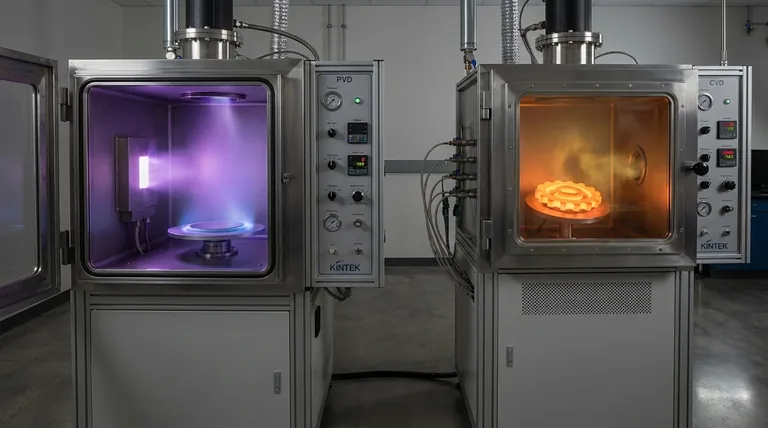
At its core, the difference between Physical Vapor Deposition (PVD) and Chemical Vapor Deposition (CVD) is how the coating material travels from its source to the surface you want to coat. PVD is a physical process, like spray painting with atoms, where a solid material is vaporized and travels in a line-of-sight to the substrate. In contrast, CVD is a chemical process where precursor gases react on the substrate's surface to grow a new solid film, much like baking a cake where ingredients transform into a new solid.
The fundamental distinction is mechanism: PVD physically transfers material from a solid source to a substrate, while CVD uses a chemical reaction from gaseous precursors to create a new material directly on the substrate. This difference dictates everything from coating uniformity to the temperatures required.
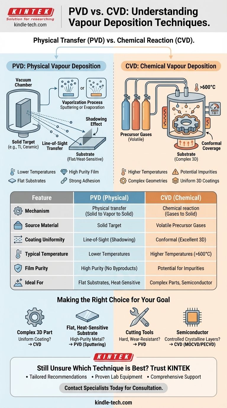
The Mechanics of Physical Vapor Deposition (PVD)
PVD is fundamentally a "line-of-sight" technique. It involves creating a vapor from a solid source material within a vacuum chamber and allowing that vapor to condense onto the substrate.
The Source Material: A Solid Target
In PVD, the material you want to deposit starts as a solid block or powder, known as a target. This could be a pure metal like titanium or a ceramic like titanium nitride.
The Vaporization Process: Sputtering vs. Evaporation
The solid target must be turned into a vapor. The two most common methods are:
- Sputtering: The target is bombarded with high-energy ions (usually an inert gas like argon), which physically knock atoms off the target's surface.
- Evaporation: The target is heated in a vacuum until it evaporates (or sublimes), creating a vapor cloud.
The Deposition Process: Straight-Line Transfer
Once vaporized, the atoms travel in a straight line through the vacuum and stick to the first surface they hit—the substrate. This is why it is called a line-of-sight process.
The Chemistry of Chemical Vapor Deposition (CVD)
CVD is fundamentally a chemical reaction process. It is not about transferring existing material but about synthesizing a new material on the substrate surface.
The Source Material: Precursor Gases
Unlike PVD's solid target, CVD starts with one or more volatile precursor gases. These gases contain the chemical elements needed for the final film.
The Reaction Process: Building a Film
These gases are introduced into a reaction chamber containing the substrate, which is typically heated. The heat provides the energy needed to trigger a chemical reaction between the precursors.
This reaction forms the desired solid material, which deposits and grows on the substrate surface. Other gaseous byproducts of the reaction are then pumped out of the chamber.
The Deposition Process: Conformal Coverage
Because the deposition happens from a gas phase that surrounds the substrate, the film can grow on all exposed surfaces simultaneously. This results in an excellent, uniform coating, even on complex 3D shapes. This is known as conformal coverage.
Understanding the Trade-offs
Choosing between PVD and CVD involves clear trade-offs tied directly to their different mechanisms.
PVD: Lower Temperatures and High Purity
PVD processes can often be performed at much lower temperatures than traditional CVD. This makes PVD ideal for coating substrates that can't withstand high heat, like plastics or certain alloys. It is also an inherently purer process as it avoids the chemical byproducts common in CVD.
CVD: Superior Conformal Coatings
CVD's greatest strength is its ability to uniformly coat intricate and complex geometries. Because the precursor gases can penetrate small cavities, CVD is unmatched for coating the inside of tubes or complex parts where a line-of-sight process would fail.
PVD: Limited by Line-of-Sight
The primary limitation of PVD is its inability to coat surfaces that are not in its direct line of sight. This creates a "shadowing" effect, making it difficult to coat undercuts, sharp corners, or the interior of complex parts uniformly.
CVD: Higher Temperatures and Potential Impurities
Many CVD processes require very high temperatures (often >600°C) to drive the necessary chemical reactions, which limits the types of substrates that can be used. Furthermore, atoms from the precursor gases (like hydrogen or chlorine) can sometimes be incorporated into the film as impurities, affecting its properties.
Making the Right Choice for Your Goal
Your application's specific requirements will determine whether PVD or CVD is the appropriate technique.
- If your primary focus is coating a complex 3D part uniformly: CVD is the superior choice due to its excellent conformal coverage.
- If your primary focus is depositing a high-purity metallic film on a flat, heat-sensitive substrate: PVD (specifically sputtering) is the ideal method.
- If your primary focus is creating a hard, wear-resistant coating on cutting tools: PVD is often preferred for its strong adhesion and lower processing temperatures, which preserve the tool's hardness.
- If your primary focus is growing highly controlled, crystalline semiconductor layers: Specialized CVD techniques (like MOCVD or PECVD) are the industry standard for their atomic-level precision.
Understanding this fundamental split between a physical transfer and a chemical reaction empowers you to select the optimal deposition technology for your specific engineering challenge.
Summary Table:
| Feature | Physical Vapor Deposition (PVD) | Chemical Vapor Deposition (CVD) |
|---|---|---|
| Mechanism | Physical transfer of material from a solid source | Chemical reaction of precursor gases on the substrate |
| Source Material | Solid target (e.g., metal, ceramic) | Volatile precursor gases |
| Coating Uniformity | Line-of-sight; potential for shadowing | Conformal; excellent for complex 3D parts |
| Typical Temperature | Lower temperatures (suitable for heat-sensitive substrates) | Higher temperatures (often >600°C) |
| Film Purity | High purity (avoids chemical byproducts) | Potential for impurities from precursor gases |
| Ideal For | Flat substrates, heat-sensitive materials, strong adhesion coatings | Complex geometries, semiconductor layers, uniform 3D coatings |
Still Unsure Which Coating Technique is Best for Your Project?
Choosing between PVD and CVD is critical for achieving the desired film properties, uniformity, and performance in your application. KINTEK, your trusted partner in laboratory equipment and consumables, specializes in providing the right deposition solutions for your specific needs.
Whether you require the high-purity, lower-temperature capabilities of PVD for sensitive substrates or the superior conformal coverage of CVD for complex 3D parts, our experts can guide you to the optimal system. We serve a wide range of laboratory needs, from R&D to production, ensuring you get the precision and reliability your work demands.
Let our expertise enhance your process:
- Tailored Recommendations: Get expert advice on selecting the ideal PVD or CVD system for your materials and application.
- Proven Performance: Benefit from our high-quality lab equipment designed for durability and precision.
- Comprehensive Support: From installation to maintenance, we ensure your deposition processes run smoothly and efficiently.
Don't leave your coating results to chance. Contact our specialists today for a personalized consultation and discover how KINTEK can empower your laboratory's success with the right deposition technology.
Visual Guide
Related Products
- HFCVD Machine System Equipment for Drawing Die Nano-Diamond Coating
- Custom CVD Diamond Coating for Lab Applications
- Chemical Vapor Deposition CVD Equipment System Chamber Slide PECVD Tube Furnace with Liquid Gasifier PECVD Machine
- RF PECVD System Radio Frequency Plasma-Enhanced Chemical Vapor Deposition RF PECVD
- 915MHz MPCVD Diamond Machine Microwave Plasma Chemical Vapor Deposition System Reactor
People Also Ask
- What is the function of tungsten filaments in HFCVD? Powering Diamond Film Synthesis with Thermal Excitation
- How expensive is chemical vapor deposition? Understanding the True Cost of High-Performance Coating
- What is the full form of HFCVD? A Guide to Hot Filament Chemical Vapor Deposition
- What is the chemical vapor deposition growth process? Build Superior Thin Films from the Atom Up
- What is the specific function of the metal filament in HF-CVD? Key Roles in Diamond Growth


