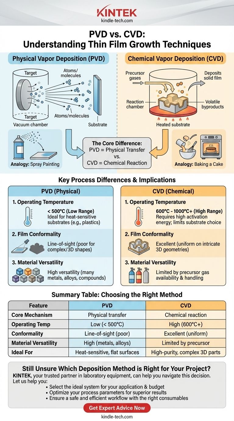
The fundamental difference between Physical Vapor Deposition (PVD) and Chemical Vapor Deposition (CVD) lies in how the coating material arrives at and forms a film on a substrate. PVD is a physical process where a solid or liquid material is vaporized and then condenses onto the target surface. In contrast, CVD is a chemical process where precursor gases are introduced into a chamber and react on a heated surface to form the desired solid film.
Choosing between PVD and CVD is not about selecting a superior technology, but about matching the process mechanism to your material requirements, desired film properties, and substrate sensitivity. The core distinction—physical transfer versus chemical reaction—dictates every major process parameter and outcome.
The Core Mechanism: Physical vs. Chemical Transformation
To understand the practical differences, you must first grasp the distinct nature of each process at the atomic level.
Physical Vapor Deposition (PVD): A Line-of-Sight Transfer
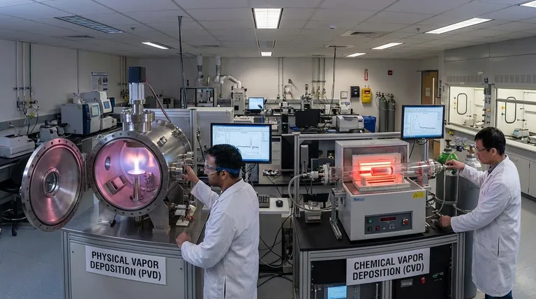
In PVD, the material to be deposited starts as a solid target in a vacuum chamber. This material is transformed into a vapor through purely physical means, such as evaporation (heating) or sputtering (bombardment with ions).
These vaporized atoms or molecules travel in a straight line through the vacuum and physically condense on the cooler substrate, forming a thin film. The material deposited is chemically identical to the source material.
Think of PVD as being analogous to spray painting. Particles of material are physically transported from a source and stick to a surface directly in their path.
Chemical Vapor Deposition (CVD): A Surface Reaction
In CVD, the coating material is introduced as one or more volatile precursor gases into a reaction chamber. These gases are not the final film material itself, but rather the chemical ingredients.
When these gases come into contact with the heated substrate, a chemical reaction is triggered. This reaction breaks down the precursor gases, depositing the desired solid material onto the substrate and creating volatile byproducts that are then pumped out of the chamber.
An effective analogy for CVD is baking a cake. Liquid ingredients (the precursor gases) react under heat to form an entirely new, solid structure (the film).
Key Process Differences and Their Implications
The fundamental distinction between a physical and chemical pathway creates significant differences in process parameters and the resulting film characteristics.
Operating Temperature
CVD processes almost always require high temperatures (typically 600°C to over 1000°C) to provide the necessary activation energy for the chemical reactions to occur on the substrate surface.
PVD processes can operate at a much lower temperature range, often below 500°C and sometimes even near room temperature. The energy is used to vaporize the source, not to drive a reaction on the substrate.
This temperature difference is often the single most important factor in choosing a method, as it dictates what substrate materials can be used without being damaged or melted.
Film Properties and Conformance
Because CVD involves a gas that can flow around an object, it produces films with excellent conformality. This means it can deposit a uniform coating over complex, three-dimensional shapes with intricate features.
PVD is a line-of-sight process. Like a shadow cast by a light, areas that are not in the direct path of the vapor source will receive little to no coating. This makes it ideal for flat surfaces but challenging for complex geometries.
Material and Substrate Versatility
PVD is extremely versatile in the materials it can deposit. Essentially, any metal, alloy, or compound that can be vaporized can be deposited.
CVD is limited to materials for which a stable, volatile precursor gas can be found or synthesized. These precursors can also be highly toxic, flammable, or corrosive, requiring specialized handling and safety protocols.
Understanding the Trade-offs
Neither method is universally better; they each represent a set of engineering compromises.
The PVD Compromise: Flexibility vs. Coverage
PVD's key advantages are its low operating temperature and its ability to deposit a vast range of materials. This makes it suitable for heat-sensitive substrates like plastics, hardened steels, and many electronic components.
The primary drawback is its poor conformality on complex parts. While substrate rotation can mitigate this, it cannot match the uniform coverage of CVD on highly intricate geometries.
The CVD Compromise: Quality vs. Constraints
CVD is renowned for producing exceptionally pure, dense, and conformal films with strong adhesion due to the high process temperatures. This makes it the gold standard for applications demanding the highest quality coatings on complex parts, such as in semiconductor manufacturing.
Its main limitations are the high heat, which restricts substrate choice, and the dependency on available precursor chemistry, which limits material options. The process can also generate hazardous byproducts that must be managed.
Making the Right Choice for Your Application
Your selection should be guided by your primary technical and operational goals.
- If your primary focus is coating complex 3D geometries or achieving maximum film purity: CVD is often the superior choice due to its excellent conformality and high-temperature process.
- If your primary focus is coating temperature-sensitive materials (like plastics or tempered steel): PVD is the necessary choice due to its lower operating temperatures.
- If your primary focus is depositing a wide variety of metallic alloys or elemental metals: PVD offers far greater flexibility and is not limited by the availability of precursor gases.
Ultimately, understanding the core physical or chemical nature of each process empowers you to select the precise tool for your specific engineering challenge.
Summary Table:
| Feature | PVD (Physical Vapor Deposition) | CVD (Chemical Vapor Deposition) |
|---|---|---|
| Core Mechanism | Physical transfer (evaporation/sputtering) | Chemical reaction on substrate |
| Operating Temperature | Low (often < 500°C) | High (typically 600°C - 1000°C+) |
| Film Conformality | Line-of-sight (poor for complex shapes) | Excellent (uniform on 3D geometries) |
| Material Versatility | High (metals, alloys, compounds) | Limited by precursor gas availability |
| Ideal For | Heat-sensitive substrates, flat surfaces | High-purity films, complex 3D parts |
Still Unsure Which Deposition Method is Right for Your Project?
Choosing between PVD and CVD is critical for achieving the desired film properties and protecting your substrate. KINTEK, your trusted partner in laboratory equipment, can help you navigate this decision.
We specialize in providing the right lab equipment and consumables for your specific thin-film deposition needs. Our experts understand the trade-offs between temperature sensitivity, material requirements, and coating conformity.
Let us help you:
- Select the ideal system for your application and budget
- Optimize your process parameters for superior results
- Ensure a safe and efficient workflow with the right consumables and support
Contact our technical specialists today for a personalized consultation. We'll work with you to ensure your thin-film deposition process is a success.
Visual Guide
Related Products
- Aluminized Ceramic Evaporation Boat for Thin Film Deposition
- Tungsten Evaporation Boat for Thin Film Deposition
- Electron Beam Evaporation Coating Oxygen-Free Copper Crucible and Evaporation Boat
- Molybdenum Tungsten Tantalum Evaporation Boat for High Temperature Applications
- Vacuum Hot Press Furnace Machine for Lamination and Heating
People Also Ask
- What is thin film deposition? Unlock Advanced Surface Engineering for Your Materials
- What is the chemical method for thin film deposition? Build Films from the Molecular Level Up
- Why are high-purity ceramic boats used for lignin activation? Ensure Purity & Thermal Stability
- What is the source of evaporation for thin film? Choosing Between Thermal and E-Beam Methods
- What are the alternatives to sputtering? Choose the Right Thin Film Deposition Method


