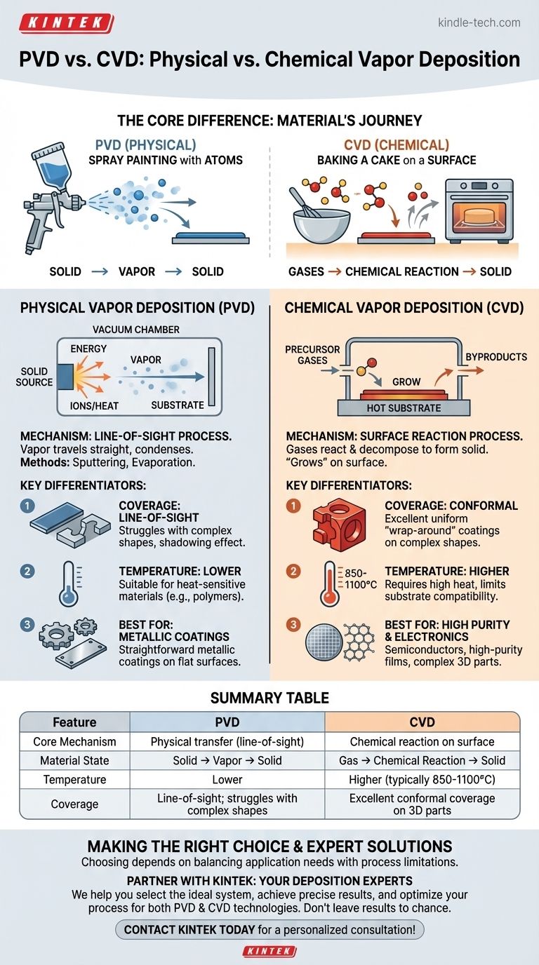
At its core, the difference is in the state of the coating material during its journey. In Physical Vapor Deposition (PVD), the material starts as a solid, is vaporized into a gas, and travels to deposit as a solid film. In Chemical Vapor Deposition (CVD), the material starts as precursor gases that undergo a chemical reaction at the surface to create a new solid film.
The central distinction is simple: PVD is a physical process, like spray painting with atoms, where material is transported in a line of sight. CVD is a chemical process, like baking a cake on a surface, where ingredients (gases) react to form a new solid layer.
The Fundamental Mechanism: Physical vs. Chemical
Understanding how each process works reveals their inherent strengths and weaknesses. The method of material transport dictates the properties of the final coating.
Physical Vapor Deposition (PVD): A Line-of-Sight Process
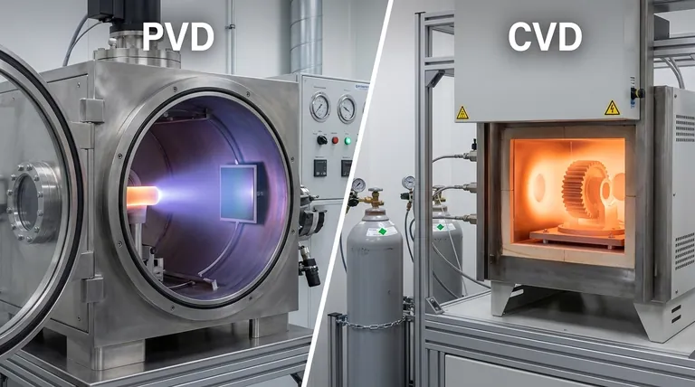
PVD is fundamentally a mechanical or thermodynamic process. A solid source material in a vacuum chamber is bombarded with energy to turn it into a vapor.
This vapor then travels in a straight line until it hits the substrate, where it condenses back into a thin, solid film. Common methods include sputtering (blasting the source with ions) and evaporation (heating the source until it boils).
Because the vapor travels in a straight line, PVD is considered a line-of-sight process. Areas not directly visible to the source material receive little to no coating.
Chemical Vapor Deposition (CVD): A Surface Reaction Process
CVD involves introducing volatile precursor gases into a reaction chamber. These gases are not the final coating material itself, but the chemical building blocks.
When these gases reach the hot substrate, they react and decompose, forming a new solid material directly on the surface. The unwanted chemical byproducts are then pumped out of the chamber.
This chemical reaction allows the film to "grow" on the surface, enabling it to coat complex shapes and internal surfaces with high uniformity.
Key Differentiators: Performance and Properties
The differences in mechanism lead to significant variations in the resulting film, affecting which process is suitable for a given application.
Conformal Coverage
CVD excels at creating uniform, "wrap-around" coatings on objects with complex geometries. The gaseous precursors can flow around and into intricate features before reacting.
PVD struggles with complex shapes due to its line-of-sight nature, often resulting in a thinner or non-existent coating on shadowed areas.
Deposition Temperature
Traditionally, CVD requires very high temperatures (often 850-1100°C) to drive the necessary chemical reactions. This high heat limits the types of substrate materials that can be coated without being damaged.
PVD processes generally operate at much lower temperatures, making them suitable for coating plastics and other heat-sensitive materials.
Film Quality and Purity
CVD can produce films of extremely high purity with excellent density and a well-defined crystal structure. This control is critical for high-performance applications like semiconductors and graphene production.
While PVD can also produce high-quality films, CVD often has an advantage in achieving low defect counts and superior crystalline alignment due to the nature of chemical growth.
Understanding the Trade-offs
Neither method is universally superior. The optimal choice depends entirely on balancing the needs of the application against the limitations of the process.
The Challenge of Substrate Compatibility
CVD's primary drawback is its high temperature requirement. Many common engineering materials, including certain steels and polymers, cannot withstand the typical heat of a CVD process without degrading.
While techniques like plasma-assisted CVD can lower the temperature, this adds complexity and cost to the operation.
The Complexity of CVD Chemistry
CVD relies on the availability of suitable precursor gases that are volatile, stable, and preferably non-toxic. Finding the right chemical recipe can be a significant challenge.
Furthermore, synthesizing films with multiple components can be difficult, as different precursors may react at different rates, leading to a non-uniform composition in the final coating.
The Limitation of PVD's Line-of-Sight
The major trade-off for PVD's lower temperature and process simplicity is its poor coverage on non-flat surfaces. This "shadowing" effect makes it unsuitable for applications requiring a perfectly uniform coating over a complex 3D part.
Making the Right Choice for Your Application
Selecting the correct deposition method requires a clear understanding of your project's primary goal.
- If your primary focus is uniform coverage on a complex 3D object: CVD is the superior choice due to its excellent conformal properties.
- If your primary focus is coating a temperature-sensitive substrate like a polymer: PVD is the clear and safer option because of its much lower operating temperature.
- If your primary focus is achieving the highest possible film purity and crystalline quality for electronics: CVD is often the leading method, as demonstrated in graphene and semiconductor manufacturing.
- If your primary focus is a straightforward metallic coating on a relatively flat surface: PVD is often a more direct and cost-effective solution.
Ultimately, your choice is a decision between the physical simplicity of PVD and the chemical precision of CVD.
Summary Table:
| Feature | PVD (Physical Vapor Deposition) | CVD (Chemical Vapor Deposition) |
|---|---|---|
| Core Mechanism | Physical transfer (line-of-sight) | Chemical reaction on surface |
| Material State | Solid → Vapor → Solid | Gas → Chemical Reaction → Solid |
| Temperature | Lower (suitable for heat-sensitive materials) | Higher (typically 850-1100°C) |
| Coverage | Line-of-sight; struggles with complex shapes | Excellent conformal coverage on 3D parts |
| Best For | Metallic coatings on flat surfaces, temperature-sensitive substrates | High-purity films, semiconductors, complex 3D parts |
Still Unsure Which Deposition Method is Right for Your Project?
Choosing between PVD and CVD is critical for achieving the desired film properties, from wear resistance to electrical conductivity. KINTEK, your trusted partner in lab equipment, specializes in providing the right deposition solutions for your specific research and production needs.
We can help you:
- Select the ideal system based on your substrate material, desired film quality, and part geometry.
- Achieve precise results with equipment tailored for high-purity semiconductor coatings or durable metallic layers.
- Optimize your process with our expertise in both PVD and CVD technologies.
Don't leave your coating results to chance. Let our experts guide you to the optimal solution for your laboratory's thin-film challenges.
Contact KINTEK today for a personalized consultation!
Visual Guide
Related Products
- Chemical Vapor Deposition CVD Equipment System Chamber Slide PECVD Tube Furnace with Liquid Gasifier PECVD Machine
- Customer Made Versatile CVD Tube Furnace Chemical Vapor Deposition Chamber System Equipment
- Split Chamber CVD Tube Furnace with Vacuum Station Chemical Vapor Deposition System Equipment Machine
- Multi Heating Zones CVD Tube Furnace Machine Chemical Vapor Deposition Chamber System Equipment
- HFCVD Machine System Equipment for Drawing Die Nano-Diamond Coating
People Also Ask
- What types of substrates are used in CVD to facilitate graphene films? Optimize Graphene Growth with the Right Catalyst
- What are the core advantages of PE-CVD in OLED encapsulation? Protect Sensitive Layers with Low-Temp Film Deposition
- What happens during deposition chemistry? Building Thin Films from Gaseous Precursors
- How are carbon nanotubes grown? Master Scalable Production with Chemical Vapor Deposition
- How expensive is chemical vapor deposition? Understanding the True Cost of High-Performance Coating


