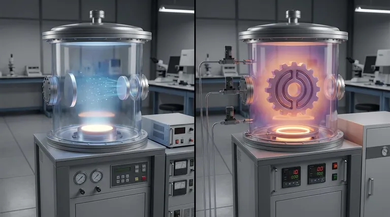
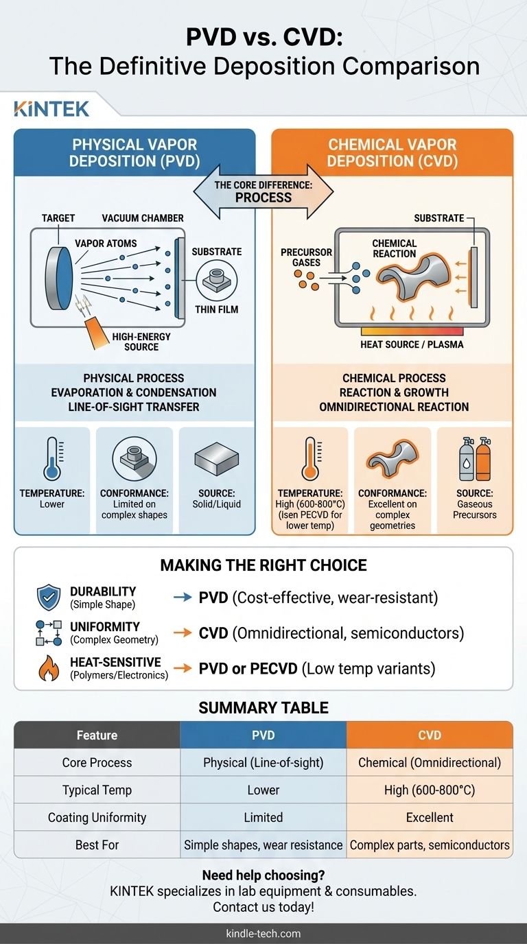
At its core, the difference is in the process. Physical Vapor Deposition (PVD) is a mechanical process that transfers a coating material from a solid source to a part's surface in a vacuum, similar to spray painting with atoms. In contrast, Chemical Vapor Deposition (CVD) uses precursor gases that trigger a chemical reaction on the part's surface, causing a new material layer to grow directly on it.
The fundamental distinction lies in how the coating material arrives and forms on the substrate. PVD is a physical, line-of-sight transfer, while CVD is an omnidirectional chemical reaction that builds the film from gaseous precursors. This single difference dictates temperature, coating uniformity, and suitable applications for each process.
The Core Mechanism: Physical vs. Chemical
To understand the practical implications of each method, you must first grasp how they fundamentally operate. The names themselves reveal the core processes.
How PVD Works: Evaporation & Condensation
PVD is a purely physical process conducted in a high vacuum. It involves vaporizing a solid material (known as the "target") using a high-energy source.
These vaporized atoms then travel in a straight line through the vacuum chamber and condense onto the substrate, forming a dense, thin film.
Common PVD methods include sputtering and ion plating. Because the material travels in a straight line, PVD is considered a line-of-sight process.
How CVD Works: Reaction & Growth
CVD involves introducing volatile precursor gases into a reaction chamber containing the substrate.
Heat (in traditional CVD) or plasma (in variants like PECVD) provides the energy needed to initiate a chemical reaction on the substrate's surface.
This reaction breaks down the gases, and the desired coating material deposits, or "grows," uniformly onto all exposed surfaces. It is not a line-of-sight process.
Key Differentiating Factors
The difference between a physical transfer and a chemical reaction creates several critical distinctions that will guide your choice of technology.
Operating Temperature
Traditional CVD is a high-temperature process, often requiring between 600°C and 800°C to drive the necessary chemical reactions.
PVD also requires high temperatures and vacuum conditions but generally operates at lower temperatures than traditional CVD.
Modern, plasma-assisted versions of CVD (such as PECVD) can operate at much lower temperatures, from room temperature to 350°C, making them suitable for heat-sensitive materials.
Coating Conformance
Because CVD is based on a chemical reaction from a gas, it coats all surfaces it can reach with exceptional uniformity. This makes it ideal for coating complex shapes and internal geometries.
PVD's line-of-sight nature means it struggles to coat shadowed areas or complex internal surfaces uniformly without sophisticated substrate rotation.
Source Material
In PVD, the coating material starts as a solid or liquid source that is physically vaporized.
In CVD, the coating material is built from one or more gaseous precursors that are introduced into the chamber.
Understanding the Trade-offs
Neither technology is universally superior. Your decision will depend on balancing the inherent advantages and limitations of each process against the requirements of your specific application.
The Temperature Limitation of CVD
The primary drawback of traditional CVD is its extremely high temperature, which can damage or warp many substrates, including plastics, certain alloys, and complex electronics.
While plasma-assisted CVD (PECVD/PACVD) solves the temperature problem, it introduces its own set of process complexities.
The "Line-of-Sight" Problem of PVD
PVD's greatest limitation is its difficulty in achieving a perfectly uniform coating on parts with complex geometries, undercuts, or deep recesses.
Overcoming this requires complex machinery to manipulate the part during deposition, which adds cost and complexity.
Equipment and Expertise
Both PVD and CVD are sophisticated processes. They require significant capital investment in vacuum chambers, power supplies, and cleanroom facilities, as well as highly skilled operators to manage the processes effectively.
Making the Right Choice for Your Goal
Your application's specific needs for temperature tolerance, geometric complexity, and coating properties will determine the correct path forward.
- If your primary focus is durability on a relatively simple shape: PVD is often an excellent and cost-effective choice, especially for wear-resistant coatings on tools.
- If your primary focus is a perfectly uniform coating on a complex geometry: CVD is superior due to its omnidirectional deposition process, making it essential in fields like semiconductor manufacturing.
- If your primary focus is coating a heat-sensitive substrate (like a polymer or electronic component): Your choice is between PVD or a low-temperature variant of CVD, such as PECVD.
Ultimately, selecting the right deposition method requires a clear understanding of your material's limits and your product's performance goals.
Summary Table:
| Feature | PVD (Physical Vapor Deposition) | CVD (Chemical Vapor Deposition) |
|---|---|---|
| Core Process | Physical transfer (line-of-sight) | Chemical reaction (omnidirectional) |
| Typical Temperature | Lower temperatures | High temperature (600-800°C) |
| Coating Uniformity | Limited on complex shapes | Excellent on complex geometries |
| Best For | Simple shapes, wear resistance | Complex parts, semiconductors |
Need help choosing the right deposition method for your application? KINTEK specializes in lab equipment and consumables, providing expert solutions for your coating challenges. Our team can help you select the ideal PVD or CVD system to meet your specific requirements for temperature, uniformity, and performance. Contact us today to discuss your project!
Visual Guide
Related Products
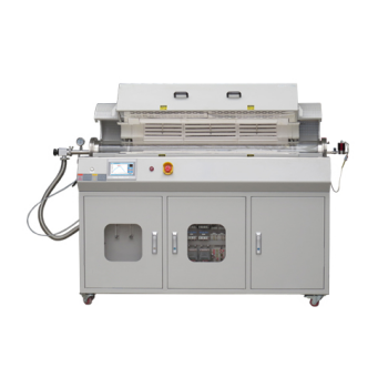
- Chemical Vapor Deposition CVD Equipment System Chamber Slide PECVD Tube Furnace with Liquid Gasifier PECVD Machine
- Inclined Rotary Plasma Enhanced Chemical Vapor Deposition PECVD Equipment Tube Furnace Machine
- RF PECVD System Radio Frequency Plasma-Enhanced Chemical Vapor Deposition RF PECVD
- Customer Made Versatile CVD Tube Furnace Chemical Vapor Deposition Chamber System Equipment
- Vacuum Hot Press Furnace Machine for Lamination and Heating
People Also Ask
- What is the difference between CVD and PVD process? A Guide to Choosing the Right Coating Method
- What is the precursor gas in PECVD? The Key to Low-Temperature Thin Film Deposition
- How plasma is generated in PECVD? A Step-by-Step Breakdown of the Process
- How are PECVD and CVD different? A Guide to Choosing the Right Thin-Film Deposition Process
- What is the difference between thermal CVD and PECVD? Choose the Right Thin-Film Deposition Method