The acronym CVD stands for Chemical Vapor Deposition. In the context of graphene, it refers to a dominant synthesis method for creating high-quality, large-area sheets of the material. The process involves growing a single, atomic layer of carbon atoms onto a catalyst substrate, typically from a carbon-containing gas like methane.
CVD is the foundational technology that makes the large-scale production of high-purity graphene feasible. It bridges the gap between lab-scale discoveries and real-world industrial applications by enabling the growth of continuous, uniform graphene films.
How CVD Graphene Growth Works
To understand why CVD is so significant, you must first understand the mechanics of the process. It's a precise, multi-step technique performed inside a controlled vacuum chamber.
The Fundamental Ingredients
The synthesis requires a few key components to succeed:
- A Catalyst Substrate: This is the surface on which the graphene will grow. Foils of copper (Cu) or nickel (Ni) are the most common catalysts.
- A Carbon Precursor: This is the source of the carbon atoms. Methane (CH₄) is a widely used gaseous precursor, though solid and liquid carbon sources can also be used.
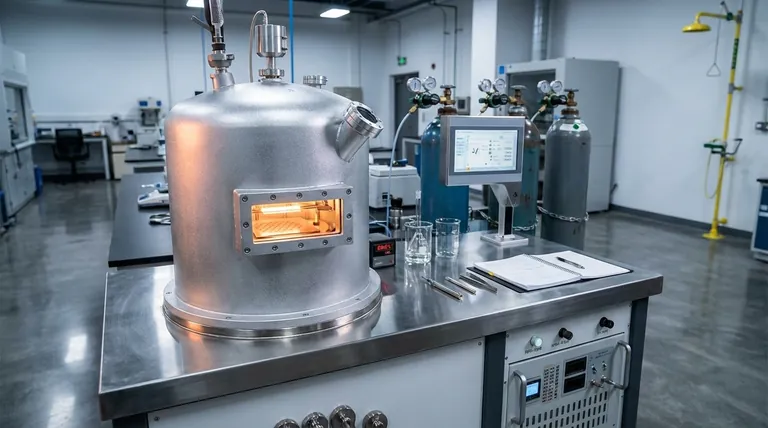
- A Controlled Environment: The process requires very high temperatures, so it is conducted in a furnace with specific carrier gases, like hydrogen (H₂) and argon (Ar), to manage the atmosphere.
The High-Temperature Process
The growth of the graphene layer follows a clear sequence of events:
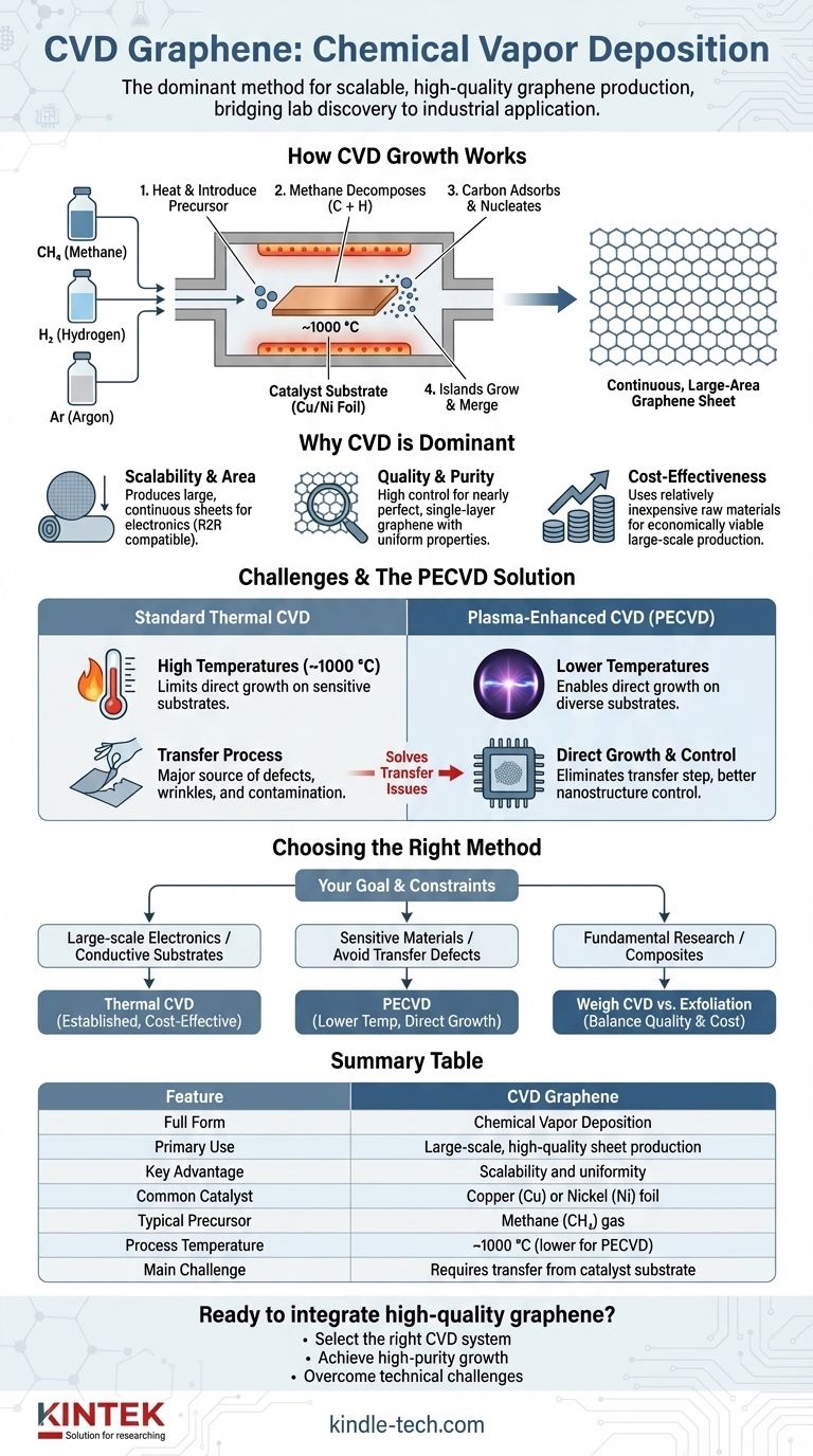
- A copper foil is heated to a high temperature, typically around 1000 °C.
- Methane gas is introduced into the chamber. At this extreme heat, the methane molecules decompose, breaking apart and releasing their carbon atoms.
- These free carbon atoms adsorb (deposit) onto the hot surface of the copper catalyst.
- The atoms diffuse across the surface and begin to nucleate, forming small, distinct crystalline islands of graphene.
- As the process continues, these islands grow and eventually merge together, forming a continuous, single-atom-thick sheet of graphene that covers the entire catalyst surface.
Why CVD is the Dominant Method
CVD is not the only way to make graphene, but it has become the most promising approach for commercial and electronic applications for several key reasons.
Scalability and Area
Unlike methods that produce small flakes, CVD can generate large, continuous sheets of graphene. This is essential for applications in electronics, where uniform coverage over a wafer or screen is required. It is the only method that shows promise for a continuous, roll-to-roll (R2R) production process.
Quality and Purity
The CVD process offers a high degree of control, allowing for the growth of nearly perfect single-layer graphene. The controlled environment and catalyst-driven growth mechanism result in a final product with high purity and structural integrity, which is critical for its unique electronic properties.
Cost-Effectiveness
While the equipment can be expensive, the raw materials (like methane and copper) are relatively inexpensive. This makes CVD a more economically viable path to large-scale graphene production compared to other, more complex synthesis strategies.
Understanding the Trade-offs and Variations
Despite its advantages, the standard CVD process has inherent challenges that have spurred the development of alternative approaches.
The Challenge of High Temperatures
The requirement for temperatures around 1000 °C means graphene cannot be grown directly on most functional materials, such as silicon wafers or flexible polymers, which cannot withstand that heat. This creates a significant integration hurdle.
The Problem of Transfer
Because the graphene is grown on a metal catalyst, it must be transferred to its final target substrate. This delicate process of lifting and moving the one-atom-thick film is a major source of defects, wrinkles, tears, and contamination, which can degrade the graphene's performance.
An Advanced Alternative: PECVD
To address these issues, Plasma-Enhanced Chemical Vapor Deposition (PECVD) was developed. By using a plasma to break down the precursor gas, PECVD offers several benefits:
- Lower Temperatures: It can operate at much lower temperatures, enabling direct growth on a wider range of substrates.
- Better Control: The plasma provides more control over the graphene's nanostructure.
- No Transfer Step: By growing graphene directly on a dielectric (insulating) substrate, PECVD can entirely eliminate the damaging transfer process, preserving the material's quality.
How to Apply This to Your Project
Your choice of graphene synthesis method depends entirely on your end goal and technical constraints.
- If your primary focus is large-scale production for electronics: Standard thermal CVD is the established, cost-effective method for creating high-quality monolayer graphene on conductive substrates.
- If your primary focus is integrating graphene onto sensitive materials or avoiding transfer-related defects: Plasma-Enhanced CVD (PECVD) is the superior choice due to its lower process temperatures and ability to grow on dielectric substrates.
- If your primary focus is fundamental research or creating composites: You must weigh the high quality and scalability of CVD against the complexity and cost of the equipment, as other methods like exfoliation might be sufficient.
Ultimately, understanding the CVD process is fundamental to appreciating how graphene moves from a theoretical wonder to a transformative industrial material.
Summary Table:
| Feature | CVD Graphene |
|---|---|
| Full Form | Chemical Vapor Deposition |
| Primary Use | Large-scale, high-quality sheet production |
| Key Advantage | Scalability and uniformity |
| Common Catalyst | Copper (Cu) or Nickel (Ni) foil |
| Typical Precursor | Methane (CH₄) gas |
| Process Temperature | ~1000 °C (lower for PECVD) |
| Main Challenge | Requires transfer from catalyst substrate |
Ready to integrate high-quality graphene into your research or product development?
The choice between thermal CVD and Plasma-Enhanced CVD (PECVD) is critical for your project's success, impacting scalability, integration, and final material quality. KINTEK specializes in providing the advanced lab equipment and expert support needed for precise graphene synthesis.
We help you:
- Select the right CVD system for your specific application (electronics, sensors, composites).
- Achieve high-purity, uniform graphene growth.
- Overcome technical challenges like substrate transfer and process optimization.
Let's discuss your graphene synthesis goals. Contact our experts today to explore the ideal solution for your laboratory needs.
Visual Guide
Related Products
- HFCVD Machine System Equipment for Drawing Die Nano-Diamond Coating
- 915MHz MPCVD Diamond Machine Microwave Plasma Chemical Vapor Deposition System Reactor
- CVD Diamond Cutting Tool Blanks for Precision Machining
- Graphite Vacuum Furnace IGBT Experimental Graphitization Furnace
- Laboratory Sterilizer Lab Autoclave Pulse Vacuum Lifting Sterilizer
People Also Ask
- What is the role of the HF-CVD system in preparing BDD electrodes? Scalable Solutions for Boron-Doped Diamond Production
- What is microwave plasma CVD? A Guide to High-Purity Diamond and Material Synthesis
- How does a Hot Filament Chemical Vapor Deposition (HFCVD) reactor function? Expert Guide to Diamond Film Fabrication
- What is the specific function of the metal filament in HF-CVD? Key Roles in Diamond Growth
- How does PACVD equipment improve DLC coatings? Unlock Low Friction and High Heat Resistance
