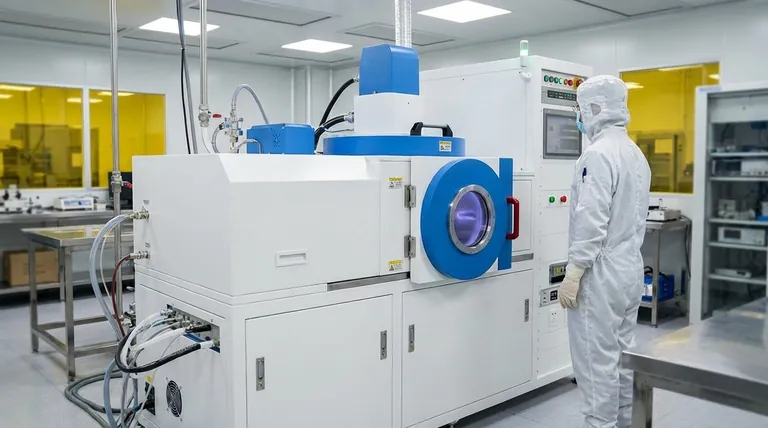
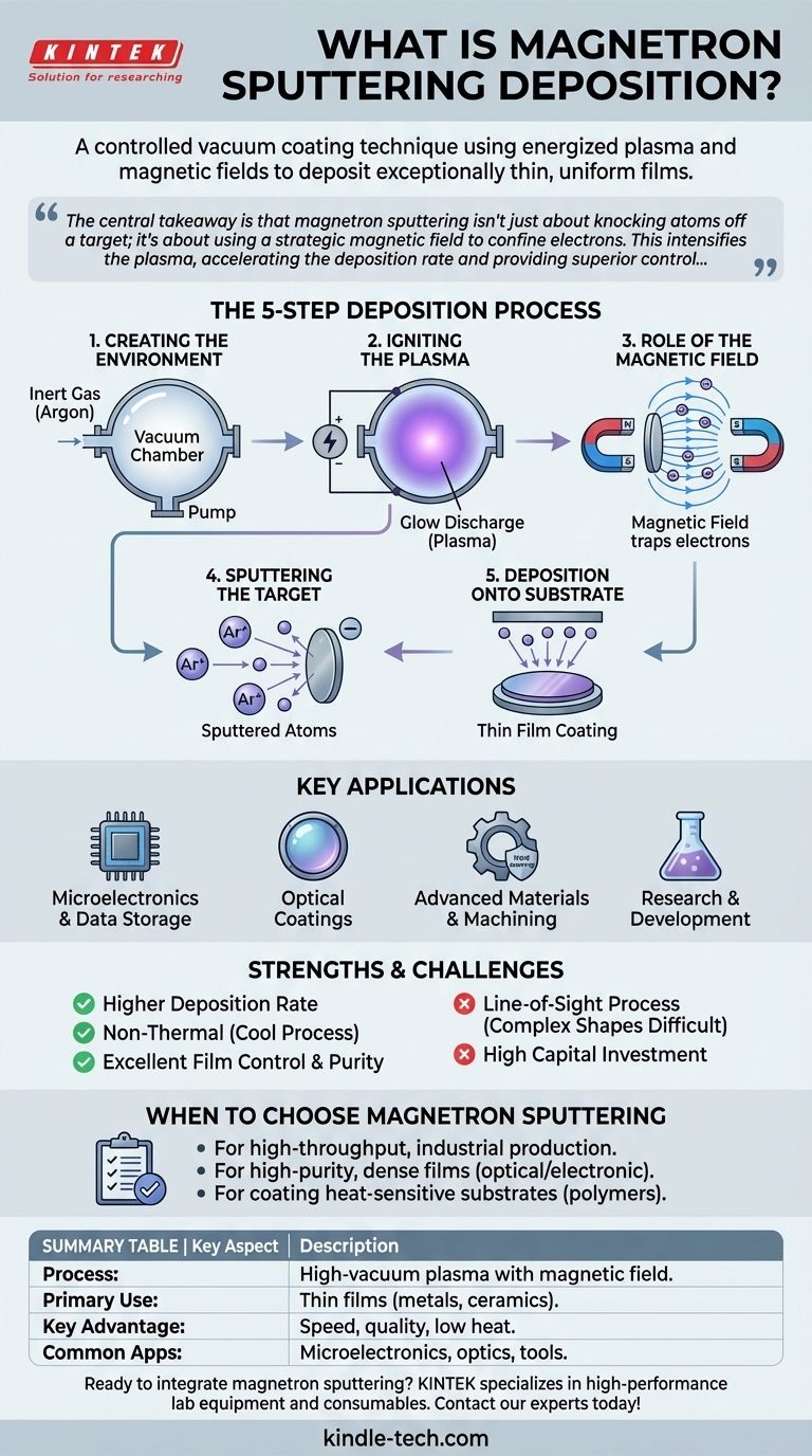
In essence, magnetron sputtering is a highly controlled vacuum coating technique used to deposit exceptionally thin, uniform films of material onto a substrate. It operates by creating an energized plasma of inert gas, which bombards a source material (the "target"). The key innovation is the use of a magnetic field—the "magnetron"—to dramatically increase the efficiency of this process, enabling faster and more stable film deposition.
The central takeaway is that magnetron sputtering isn't just about knocking atoms off a target; it's about using a strategic magnetic field to confine electrons. This intensifies the plasma, accelerating the deposition rate and providing superior control over the final film's properties compared to standard sputtering methods.
How Magnetron Sputtering Works: A Step-by-Step Breakdown
To understand this process, it's best to visualize it as a sequence of controlled events occurring within a vacuum chamber.
1. Creating the Environment
First, a high vacuum is created in a sealed chamber. This removes unwanted particles that could contaminate the film.
The chamber is then backfilled with a small, controlled amount of an inert gas, most commonly argon. This gas provides the ions needed for the sputtering process.
2. Igniting the Plasma
A high voltage is applied across the chamber, with the target material acting as the cathode (negative electrode). This electrical energy strips electrons from the argon gas atoms.
This creates a plasma, a partially ionized gas consisting of positive argon ions and free electrons. This plasma is often visible as a characteristic colorful glow, known as a "glow discharge."
3. The Role of the Magnetic Field
This is the critical step that defines magnetron sputtering. A powerful magnetic field is configured behind the target.
This magnetic field traps the much lighter electrons, forcing them to move in a complex spiral path near the surface of the target. This greatly increases the probability that an electron will collide with and ionize a neutral argon atom.
The result is a dense, stable plasma concentrated directly in front of the target, which is essential for an efficient process.
4. Sputtering the Target
The positively charged argon ions in the plasma are accelerated by the electric field and smash into the negatively charged target material with tremendous force.
This high-energy bombardment physically knocks out, or "sputters," individual atoms from the target surface. These neutral atoms are ejected into the vacuum chamber.
5. Deposition onto the Substrate
The ejected target atoms travel through the low-pressure environment until they strike the substrate—the object being coated.
Upon arrival, these atoms condense on the substrate's surface, gradually building up a thin, highly uniform film.
Key Applications Across Industries
The precision and versatility of magnetron sputtering have made it a vital technology in numerous high-performance fields.
Microelectronics and Data Storage
This is one of its most common uses. It is essential for depositing the thin metallic and insulating layers required for manufacturing integrated circuits and computer hard disks.
Optical Coatings
The process is ideal for creating specialized optical films, such as anti-reflection coatings on lenses, low-emissivity (Low-E) films on architectural glass to improve insulation, and translucent or reflective decorative layers.
Advanced Materials and Machining
In industrial applications, magnetron sputtering is used to apply super-hard coatings to cutting tools, increasing their lifespan and performance. It's also used for creating self-lubricating films on mechanical components to reduce friction.
Research and Development
The technology is a cornerstone of materials science research, enabling the creation of novel thin films for applications like solar cells, high-temperature superconductors, and advanced memory alloys.
Understanding the Strengths and Limitations
Like any advanced manufacturing process, magnetron sputtering has distinct advantages and practical considerations. Being aware of these is key to determining its suitability for a given task.
The Primary Advantages
The magnetic confinement of the plasma leads to a higher deposition rate than non-magnetron methods, making it more suitable for industrial production.
It is a non-thermal coating technology, meaning the substrate does not get significantly hot. This allows for the coating of heat-sensitive materials like plastics and polymers without causing damage.
The process offers exceptional control over film thickness, purity, and uniformity, resulting in high-quality, dense coatings with excellent adhesion.
Potential Challenges and Considerations
Magnetron sputtering is a line-of-sight process. Atoms travel in a relatively straight line from the target to the substrate, which can make it challenging to uniformly coat complex, three-dimensional shapes.
The equipment required—including vacuum chambers, high-voltage power supplies, and magnetrons—represents a significant capital investment and requires specialized knowledge to operate and maintain.
When to Choose Magnetron Sputtering
Your decision to use this method should be driven by the specific requirements of your final product.
- If your primary focus is high-throughput production: Magnetron sputtering's high deposition rates make it ideal for industrial-scale applications requiring speed and efficiency.
- If your primary focus is creating high-purity, dense films: The controlled plasma environment ensures excellent film quality for demanding optical or electronic uses.
- If your primary focus is coating heat-sensitive substrates like polymers: Its non-thermal nature prevents damage to the underlying material, making it a superior choice over high-temperature methods.
Ultimately, magnetron sputtering stands as a cornerstone technology for engineering surfaces with precise, functional properties at the atomic level.
Summary Table:
| Key Aspect | Description |
|---|---|
| Process | High-vacuum plasma deposition using a magnetic field to enhance efficiency. |
| Primary Use | Coating substrates with thin, uniform films of metals, alloys, or ceramics. |
| Key Advantage | High deposition rates, excellent film quality, and low substrate heating. |
| Common Applications | Microelectronics, optical coatings, hard coatings for tools, and R&D. |
Ready to integrate magnetron sputtering into your lab workflow? KINTEK specializes in high-performance lab equipment and consumables, providing reliable sputtering systems tailored to your research or production needs. Whether you're developing next-generation electronics, durable industrial coatings, or innovative optical films, our expertise ensures you achieve precise, reproducible results. Contact our experts today to discuss how our solutions can enhance your thin film deposition process!
Visual Guide
Related Products
- Spark Plasma Sintering Furnace SPS Furnace
- RF PECVD System Radio Frequency Plasma-Enhanced Chemical Vapor Deposition RF PECVD
People Also Ask
- What is the process fundamentals of spark plasma sintering? Achieve Rapid, High-Density Material Consolidation
- What is SPS sintering method? A Guide to High-Speed, High-Performance Material Fabrication
- What is the mechanism of SPS process? A Deep Dive into Rapid, Low-Temperature Sintering
- What are the advantages of CAMI/SPS for W-Cu composite preparation? Reduce cycles from hours to seconds.
- What is the theory of spark plasma sintering? A Guide to Rapid, Low-Temperature Densification

