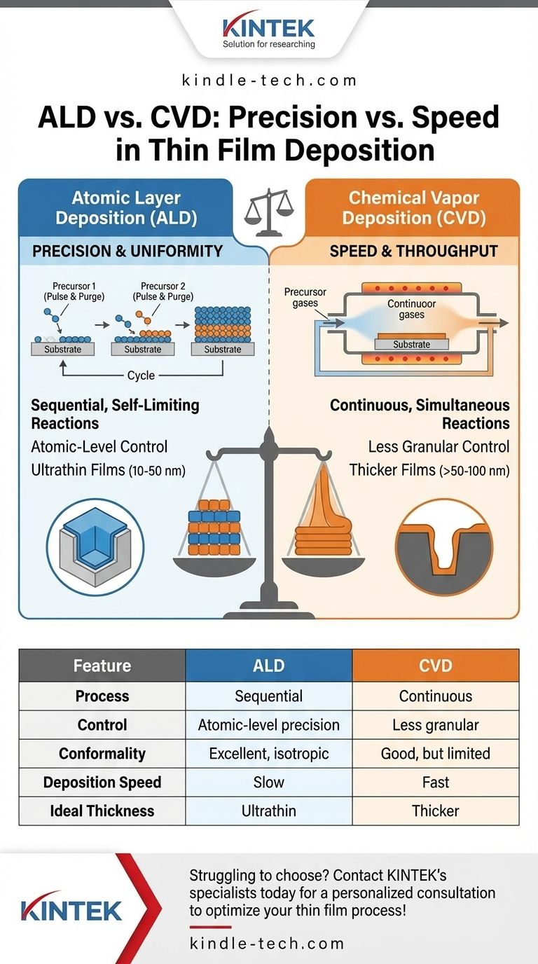
The fundamental difference between Atomic Layer Deposition (ALD) and Chemical Vapor Deposition (CVD) lies in their reaction mechanisms. ALD builds films one atomic layer at a time through sequential, self-limiting chemical reactions, offering unparalleled precision. CVD, in contrast, uses a continuous, simultaneous reaction of precursor gases, enabling much faster deposition rates.
The choice between ALD and CVD hinges on a critical trade-off: precision versus speed. ALD provides atomic-level control for complex and ultrathin films, while CVD offers higher throughput for thicker layers where absolute precision is less critical.
The Mechanics of Deposition: Sequential vs. Continuous
To understand the practical differences, we must first examine how each process works at a fundamental level. The core distinction is whether the chemical reactions happen sequentially or all at once.
How CVD Works: A Continuous Reaction
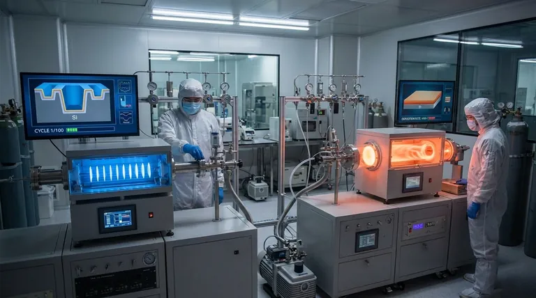
In a Chemical Vapor Deposition (CVD) process, all precursor gases are introduced into the reaction chamber simultaneously.
These gases react together on and above the heated substrate, leading to a continuous deposition of the desired thin film. This process is fast and efficient for growing relatively thick layers of material.
How ALD Works: A Separated, Self-Limiting Process
Atomic Layer Deposition (ALD) is a more controlled, cyclical variant of CVD. It breaks the overall reaction into two or more separate half-reactions.
First, one precursor gas is pulsed into the chamber, where it forms a single, self-limiting atomic layer on the substrate. Any excess gas is purged. Then, a second precursor is pulsed in to react with the first layer, completing the material deposition for that cycle before it too is purged. This cycle repeats to build the film layer by atomic layer.
Key Differentiators in Practice
The mechanical differences between these two methods lead to distinct outcomes in film quality, coverage, and speed.
Film Thickness and Control
ALD offers atomic-level precision in controlling film thickness. Because the film is built one monolayer at a time, you can achieve a specific thickness with extreme accuracy, making it ideal for the ultrathin films (10-50 nm) required in modern electronics.
CVD provides less granular control but is perfectly suitable for applications requiring thicker films where nanometer-level precision is unnecessary.
Conformality and Coverage
Conformality refers to a film's ability to coat uneven surfaces and complex 3D structures uniformly.
ALD provides near-perfect, isotropic conformality. Its self-limiting nature ensures that every surface, including deep trenches and high-aspect-ratio structures, is coated evenly. This is a significant advantage over "line-of-sight" methods like physical vapor deposition (PVD).
While CVD offers good conformality, it can struggle to maintain uniform thickness inside very complex or deep structures compared to ALD.
Deposition Rate
The most significant advantage of CVD is its high deposition rate. Since the reaction is continuous, films can be grown much more quickly.
ALD is an inherently slow process. The repeated cycles of pulsing and purging limit its throughput, making it less practical for applications demanding thick films or high-volume production.
Understanding the Trade-offs
Choosing between ALD and CVD requires weighing their respective strengths and weaknesses against your specific goals.
The Precision of ALD
The primary advantage of ALD is its unparalleled control over film thickness, density, and uniformity. This precision is non-negotiable for fabricating advanced semiconductor devices and other nanoscale technologies.
The Speed of CVD
The main benefit of CVD is its speed and efficiency, which translates to higher throughput and often lower cost. It is the workhorse for many industrial applications where thick, functional coatings are needed without atomic-level specifications.
Material and Process Complexity
CVD technology is generally more mature, with a wider range of established precursors and processes for various materials. Developing a new ALD process can be more complex and time-consuming due to the precise requirements of its self-limiting chemistry.
Making the Right Choice for Your Application
Your decision will be dictated by the specific technical and economic requirements of your project.
- If your primary focus is ultrathin, perfectly uniform films on complex 3D structures: ALD is the superior and often the only viable choice due to its atomic-level control.
- If your primary focus is depositing thicker films quickly and economically: CVD offers the necessary speed, efficiency, and scalability for the job.
- If your project requires a balance of good coverage and reasonable speed: CVD is frequently the more practical and cost-effective starting point for films thicker than 50-100 nm.
Understanding this fundamental difference between sequential precision and continuous speed empowers you to select the optimal deposition technique for your goal.
Summary Table:
| Feature | Atomic Layer Deposition (ALD) | Chemical Vapor Deposition (CVD) |
|---|---|---|
| Process | Sequential, self-limiting reactions | Continuous, simultaneous reactions |
| Control | Atomic-level precision | Less granular control |
| Conformality | Excellent, isotropic (uniform on complex 3D structures) | Good, but can struggle with high-aspect-ratio structures |
| Deposition Speed | Slow (layer-by-layer) | Fast (continuous) |
| Ideal Film Thickness | Ultrathin films (10-50 nm) | Thicker films (>50-100 nm) |
| Primary Advantage | Precision and uniformity | Speed and throughput |
Struggling to choose the right deposition technique for your lab's specific needs? The choice between ALD's atomic-level precision and CVD's high-speed deposition is critical for your research and production outcomes. At KINTEK, we specialize in providing high-quality lab equipment and consumables tailored to your laboratory's unique requirements. Our experts can help you select the ideal system to achieve perfect film uniformity or maximize your throughput. Let's optimize your thin film process together – contact our specialists today for a personalized consultation!
Visual Guide
Related Products
- CVD Diamond for Thermal Management Applications
- CVD Diamond Optical Windows for Lab Applications
- CVD Diamond Dressing Tools for Precision Applications
- CVD Diamond Domes for Industrial and Scientific Applications
- Laboratory CVD Boron Doped Diamond Materials
People Also Ask
- What is the chemical vapour deposition method for diamonds? Grow a Diamond from a Gas
- What are the characteristics of CVD diamond? Unlocking Superior Performance for Industrial Tools
- How long does it take to make a CVD diamond? A Detailed Look at the Growth Timeline
- What is the hardness of CVD diamond? The Ultimate Guide to Engineered Super-Materials
- Will a CVD diamond pass a diamond tester? Yes, because it's a real diamond.


