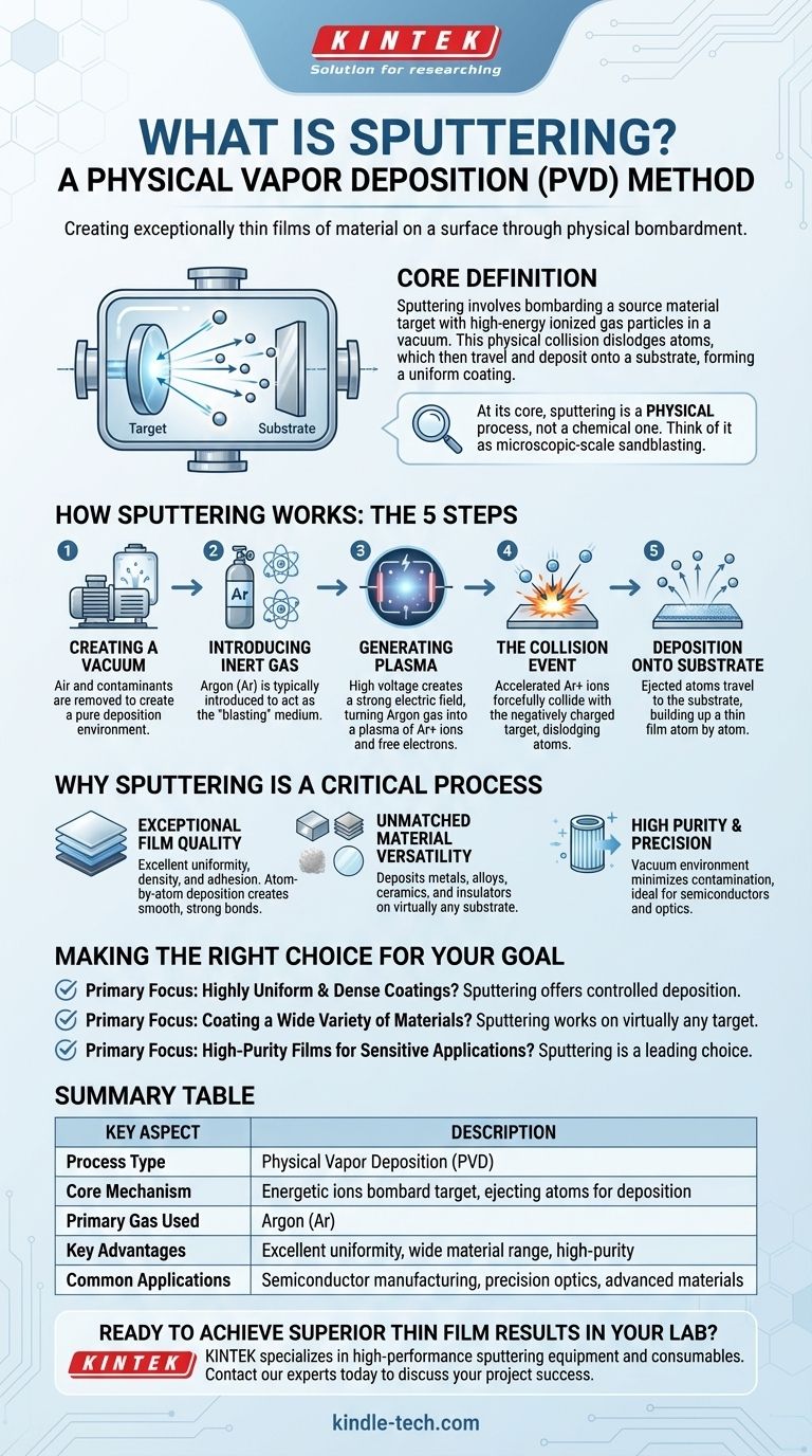
In a technical context, sputtering is a physical vapor deposition (PVD) method used to create exceptionally thin films of material on a surface. The process involves bombarding a source material, called a target, with high-energy ionized gas particles in a vacuum. This collision physically dislodges, or "sputters," atoms from the target, which then travel and deposit onto a nearby object, known as a substrate, forming a uniform coating.
At its core, sputtering is a physical process, not a chemical one. Think of it as a microscopic-scale sandblasting where individual atoms are knocked loose from a source material by energetic ions and then precisely re-deposited as an ultra-thin, high-quality film onto another surface.

How Sputtering Works: The Core Mechanism
Sputtering is a highly controlled process that takes place inside a sealed vacuum chamber. The fundamental steps are consistent across most applications.
Step 1: Creating a Vacuum
First, a vacuum is created inside a deposition chamber. This removes air and other particles that could contaminate the thin film or interfere with the process.
Step 2: Introducing an Inert Gas
An inert gas, most commonly Argon (Ar), is introduced into the chamber. This gas will not react chemically with the target material; it will only act as the "blasting" medium.
Step 3: Generating a Plasma
A high voltage is applied within the chamber, creating a strong electric field. This voltage strips electrons from the Argon atoms, turning the gas into a plasma—an energized state of matter consisting of positive ions (Ar+) and free electrons.
Step 4: The Collision Event
The positively charged Argon ions are forcefully accelerated toward the negatively charged source material, or target. They collide with the target's surface with significant momentum and energy.
Step 5: Deposition onto the Substrate
This high-energy impact physically knocks atoms or molecules out of the target material. These ejected particles travel in a straight line through the vacuum and land on the substrate (the object being coated), gradually building up a thin film one atom at a time.
Why Sputtering is a Critical Process
The characteristics of the films produced by sputtering make it an invaluable technique across numerous high-tech industries. It offers a unique combination of control, quality, and versatility.
Exceptional Film Quality
Sputtering produces films with excellent uniformity, density, and adhesion. Because the material is deposited atom by atom, the resulting coating is smooth and bonds strongly to the substrate.
Unmatched Material Versatility
The process is purely physical, which means it can be used to deposit a vast range of materials. This includes metals, alloys, ceramics, and even insulating materials on virtually any type of substrate.
High Purity and Precision
The vacuum environment is critical for creating high-purity coatings free from contamination. This makes sputtering ideal for sensitive applications like semiconductor manufacturing and precision optics where even tiny impurities can cause failure.
Making the Right Choice for Your Goal
Understanding the outcome of sputtering helps clarify when it is the superior choice for a manufacturing or research challenge.
- If your primary focus is creating highly uniform and dense coatings: Sputtering is an ideal method due to its controlled, atom-by-atom deposition process.
- If your primary focus is coating a wide variety of materials, including non-conductors: Sputtering offers a significant advantage as its physical mechanism works on virtually any target material.
- If your primary focus is high-purity films for sensitive applications like semiconductors or optics: The vacuum environment and physical nature of sputtering make it a leading choice for minimizing contamination.
Ultimately, sputtering is a precise and powerful engineering tool for building advanced materials from the atomic level up.
Summary Table:
| Key Aspect | Description |
|---|---|
| Process Type | Physical Vapor Deposition (PVD) |
| Core Mechanism | Energetic ions bombard a target, physically ejecting atoms to deposit on a substrate. |
| Primary Gas Used | Argon (Ar) |
| Key Advantages | Excellent film uniformity, density, adhesion; works with a wide range of materials (metals, ceramics, insulators); high-purity coatings. |
| Common Applications | Semiconductor manufacturing, precision optics, advanced materials research. |
Ready to achieve superior thin film results in your lab?
KINTEK specializes in high-performance sputtering equipment and consumables, delivering the precision and reliability your research and development demands. Our solutions are engineered for exceptional film quality, material versatility, and high-purity outcomes.
Contact our experts today to discuss how our sputtering systems can enhance your laboratory's capabilities and accelerate your project success.
Visual Guide
Related Products
- RF PECVD System Radio Frequency Plasma-Enhanced Chemical Vapor Deposition RF PECVD
- HFCVD Machine System Equipment for Drawing Die Nano-Diamond Coating
- 915MHz MPCVD Diamond Machine Microwave Plasma Chemical Vapor Deposition System Reactor
- Vacuum Hot Press Furnace Machine for Lamination and Heating
- Laboratory Sterilizer Lab Autoclave Pulse Vacuum Lifting Sterilizer
People Also Ask
- What is plasma activated chemical vapour deposition method? A Low-Temperature Solution for Advanced Coatings
- What is an example of PECVD? RF-PECVD for High-Quality Thin Film Deposition
- How are PECVD and CVD different? A Guide to Choosing the Right Thin-Film Deposition Process
- Why is PECVD environment friendly? Understanding the Eco-Friendly Benefits of Plasma-Enhanced Coating
- What are the advantages of PECVD? Enable Low-Temperature, High-Quality Thin-Film Deposition


