While there is no single "most common" method for all nanomaterials, the landscape is dominated by two major approaches: wet-chemical synthesis and vapor deposition. Methods like the sol-gel process are extremely common for producing large quantities of oxide nanoparticles due to their low cost and scalability. In parallel, Chemical Vapor Deposition (CVD) is the most widely employed technique for creating high-purity thin films and specific structures like carbon nanotubes.
The "best" or "most common" synthesis method is entirely dependent on the target material, its desired form (e.g., powder vs. film), and the required balance between cost, quality, and scale. Understanding this context is more valuable than searching for a single answer.
The Two Fundamental Approaches to Synthesis
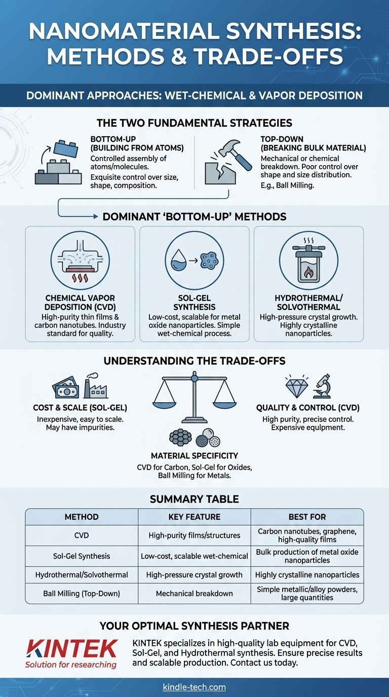
To understand nanomaterial synthesis, it's best to categorize methods into two foundational strategies: building up from atoms (bottom-up) or carving down from bulk material (top-down).
Bottom-Up: Building from the Atom Up
This is the most common and versatile strategy. It involves the controlled assembly of atoms or molecules to form nanostructures. This provides exquisite control over size, shape, and composition.
Nearly all of the most frequently used methods, including chemical and vapor deposition, fall into this category.
Top-Down: Breaking Down Bulk Material
This approach starts with a larger, bulk material and uses mechanical or chemical force to break it down into nanoscale particles.
A primary example is ball milling, where a material is ground into a fine powder inside a rotating chamber with milling balls. While effective for producing large quantities of simple nanoparticles, this method offers poor control over particle shape and size distribution.
A Closer Look at Dominant "Bottom-Up" Methods
Most innovation and application-specific work happens with bottom-up techniques due to their precision. The following methods are pillars of the field.
Chemical Vapor Deposition (CVD): The Standard for Purity and Films
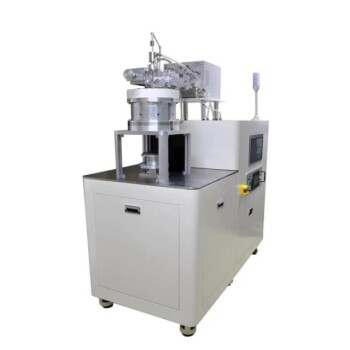
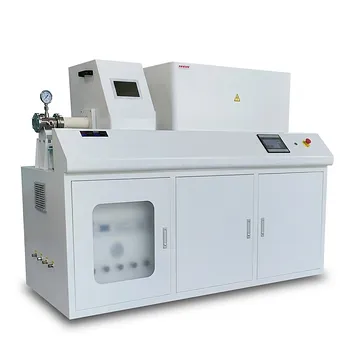
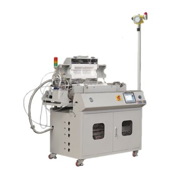
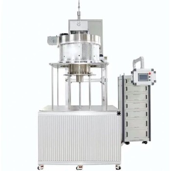
CVD involves flowing a precursor gas over a heated substrate. The gas reacts or decomposes on the substrate's surface, depositing a high-quality, solid thin film or growing nanostructures.
It is the dominant method for producing high-purity films and is one of the most common techniques for synthesizing carbon nanomaterials, such as nanotubes and graphene.
Sol-Gel Synthesis: The Workhorse for Oxides
The sol-gel process is a low-temperature, wet-chemical technique. It starts with a chemical solution (the "sol") that evolves into a gel-like network containing the desired molecules.
After drying and heat treatment, this gel is converted into a solid material. It is exceptionally popular for fabricating metal oxide nanoparticles at a large scale due to its low cost and procedural simplicity.
Hydrothermal and Solvothermal Methods: Control Through Pressure
These are variations of wet-chemical synthesis where the reaction takes place in a sealed, heated vessel (an autoclave), often under high pressure.
Using water as the solvent is known as the hydrothermal method, while using other solvents is called solvothermal. The high temperature and pressure can promote the growth of highly crystalline nanoparticles, offering excellent control over the final structure.
Understanding the Trade-offs
Choosing a synthesis method is a matter of balancing competing priorities. No single technique is superior in all aspects.
Cost vs. Quality
Wet-chemical methods like sol-gel are generally inexpensive and easy to scale up, making them ideal for bulk production. However, they may result in more impurities or a wider size distribution.
Conversely, methods like CVD require sophisticated vacuum equipment and are more expensive, but they produce materials of exceptionally high purity and structural quality.
Control vs. Scalability
Bottom-up methods like CVD and hydrothermal synthesis offer precise control over the size, shape, and crystal structure of the nanomaterials.
Top-down methods like ball milling, while easily scalable, provide very little control over particle morphology. This makes them unsuitable for applications requiring uniform, well-defined nanoparticles.
Material Specificity
Some methods are inherently better suited for certain materials. CVD excels with carbon-based nanomaterials. Sol-gel is the go-to for a vast range of metal oxides. Other methods, like laser ablation, are common for producing carbon and metallic nanoparticles.
Making the Right Choice for Your Goal
Your choice of synthesis method should be driven by your end goal.
- If your primary focus is high-purity thin films or carbon nanotubes: Chemical Vapor Deposition (CVD) is the established industry-standard technique.
- If your primary focus is cost-effective, large-scale production of oxide nanoparticles: The sol-gel or hydrothermal methods are your most practical and widely used options.
- If your primary focus is creating simple metallic or alloy powders without complex chemistry: Top-down mechanical methods like ball milling offer a direct and scalable route.
Ultimately, understanding the core principles and trade-offs of these key methods is the critical first step toward successful nanomaterial fabrication.
Summary Table:
| Method | Key Feature | Best For |
|---|---|---|
| Chemical Vapor Deposition (CVD) | High-purity thin films & structures | Carbon nanotubes, graphene, high-quality films |
| Sol-Gel Synthesis | Low-cost, scalable wet-chemical process | Bulk production of metal oxide nanoparticles |
| Hydrothermal/Solvothermal | High-pressure crystal growth | Highly crystalline nanoparticles |
| Ball Milling (Top-Down) | Mechanical breakdown of bulk material | Simple metallic/alloy powders, large quantities |
Ready to select the optimal synthesis method for your nanomaterials? The right lab equipment is critical for success. KINTEK specializes in high-quality lab equipment and consumables, from CVD systems to reactors for sol-gel and hydrothermal synthesis. Our expertise ensures you get the precise tools needed for high-purity results and scalable production. Contact us today to discuss your specific laboratory needs and how we can support your research and development goals.
Visual Guide
Related Products
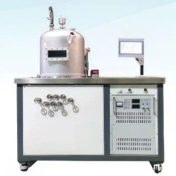
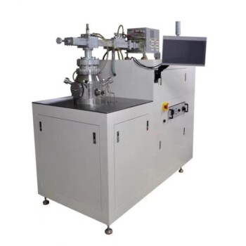
- HFCVD Machine System Equipment for Drawing Die Nano-Diamond Coating
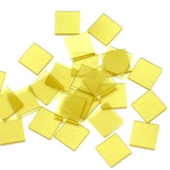
- Laboratory CVD Boron Doped Diamond Materials
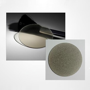
- CVD Diamond for Thermal Management Applications
- Custom CVD Diamond Coating for Lab Applications
- CVD Diamond Optical Windows for Lab Applications
People Also Ask
- What are the disadvantages and challenges of the HFCVD method? Overcome Growth Limits and Filament Issues
- What is the function of tungsten filaments in HFCVD? Powering Diamond Film Synthesis with Thermal Excitation
- What are the advantages of chemical vapor deposition? Achieve Superior Thin Films for Your Lab
- Why is Chemical Vapor Deposition (CVD) equipment uniquely suited for constructing hierarchical superhydrophobic structures?
- What is the chemical vapor deposition growth process? Build Superior Thin Films from the Atom Up
