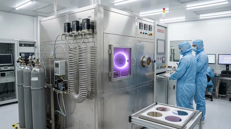
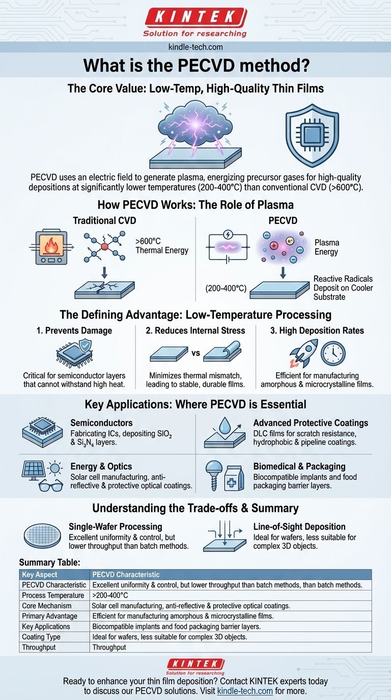
Plasma-Enhanced Chemical Vapor Deposition (PECVD) is a process used to deposit high-quality, uniform thin films onto a substrate at significantly lower temperatures than conventional methods. It achieves this by using an electric field to generate a plasma, which energizes the precursor gases and allows them to react and form the desired film without requiring extreme heat.
The core value of PECVD is its ability to perform high-quality depositions at low temperatures. This makes it an indispensable technology for fabricating modern electronics and coating temperature-sensitive materials that would be damaged or destroyed by traditional high-heat processes.
How PECVD Works: The Role of Plasma
Harnessing Plasma for Deposition
In traditional Chemical Vapor Deposition (CVD), high temperatures (often >600°C) are used to provide the energy needed to break down precursor gases and initiate a chemical reaction on the substrate surface.
PECVD fundamentally changes this equation. Instead of relying solely on thermal energy, it introduces energy via an electric field, which ionizes the precursor gases and creates a plasma (a state of matter containing ions and electrons).
Enabling Low-Temperature Reactions
This plasma is highly reactive. The energetic particles within it break down the precursor gases into reactive radicals, which are then deposited onto the cooler substrate surface.
Because the plasma provides the necessary reaction energy, the substrate itself can be kept at a much lower temperature (typically 200-400°C). This is the defining characteristic of the entire process.
The Defining Advantage: Low-Temperature Processing
Preventing Damage to Sensitive Components
The low-temperature nature of PECVD is critical in the semiconductor industry. Integrated circuits contain delicate, previously fabricated layers that cannot withstand the high temperatures of other deposition methods. PECVD allows for the deposition of insulating or conductive films without damaging the underlying device.
Reducing Internal Material Stress
When materials with different thermal expansion rates are heated and cooled together, it creates internal stress that can cause films to crack or delaminate.
By minimizing the process temperature, PECVD significantly reduces this thermal mismatch, resulting in more stable and durable films with less internal stress.
Achieving High Deposition Rates
For certain materials, such as amorphous and microcrystalline films, PECVD can achieve a relatively high deposition rate. This efficiency is crucial for manufacturing processes where throughput is a key consideration.
Where PECVD is Essential: Key Applications
Semiconductor Manufacturing
PECVD is a cornerstone of fabricating integrated circuits. It is widely used to deposit essential insulating layers, such as silicon dioxide (SiO₂) and silicon nitride (Si₃N₄), that isolate conductive pathways within a microchip.
Advanced Protective Coatings
The method is used to create highly durable and functional surface coatings. This includes creating Diamond-Like Carbon (DLC) films for scratch resistance, hydrophobic coatings for water repellency, and protective layers for mechanical parts and even oil pipelines.
Energy and Optics
In the photovoltaic industry, PECVD is essential for manufacturing solar cells. It is also used to apply anti-reflective and protective optical coatings for products ranging from eyeglasses to precision scientific instruments.
Biomedical and Packaging
The biocompatibility and protective qualities of PECVD films make them suitable for coating medical implants. The technology is also used to create barrier layers in the food packaging industry to improve shelf life.
Understanding the Trade-offs
Single-Wafer Processing
A key operational characteristic of PECVD is that it is typically a single-wafer process. This allows for excellent uniformity and control over the film deposited on an individual substrate.
However, this contrasts with other methods like Low-Pressure CVD (LPCVD), which can often process large batches of wafers simultaneously. The choice between them often depends on whether the priority is per-wafer quality control or high-volume throughput.
Line-of-Sight Deposition
PECVD is a single-sided coating method. The plasma and precursor gases are directed toward one surface of the substrate. This is ideal for semiconductor wafers but makes it less suitable for uniformly coating complex, three-dimensional objects on all sides at once.
Making the Right Choice for Your Goal
The decision to use PECVD is driven by the specific requirements of the substrate and the desired film properties.
- If your primary focus is processing temperature-sensitive materials: PECVD is the definitive choice, as its low-temperature operation prevents damage to delicate components like integrated circuits.
- If your primary focus is creating durable functional coatings: PECVD is an excellent method for depositing high-performance films like DLC or hydrophobic layers on a wide range of substrates.
- If your primary focus is high-throughput batch processing for non-sensitive materials: Other methods like LPCVD might be a more efficient alternative, though they lack the low-temperature advantage.
Ultimately, PECVD is a powerful and versatile tool that enables the creation of advanced materials and devices that would otherwise be impossible to fabricate.
Summary Table:
| Key Aspect | PECVD Characteristic |
|---|---|
| Process Temperature | 200-400°C (significantly lower than conventional CVD) |
| Core Mechanism | Uses plasma to energize precursor gases |
| Primary Advantage | Enables deposition on temperature-sensitive substrates |
| Key Applications | Semiconductor manufacturing, solar cells, protective coatings, medical implants |
| Coating Type | Single-sided, line-of-sight deposition |
| Throughput | Typically single-wafer processing (excellent uniformity) |
Ready to enhance your thin film deposition capabilities?
KINTEK specializes in advanced lab equipment and consumables for cutting-edge deposition technologies. Whether you're working with sensitive semiconductor materials, developing solar cells, or creating specialized protective coatings, our expertise in PECVD solutions can help you achieve superior results while protecting your temperature-sensitive substrates.
Contact our experts today to discuss how our PECVD equipment and support can advance your research and manufacturing processes. Let us help you unlock the potential of low-temperature, high-quality thin film deposition for your specific application.
Visual Guide
Related Products
- Inclined Rotary Plasma Enhanced Chemical Vapor Deposition PECVD Equipment Tube Furnace Machine
- Chemical Vapor Deposition CVD Equipment System Chamber Slide PECVD Tube Furnace with Liquid Gasifier PECVD Machine
- Inclined Rotary Plasma Enhanced Chemical Vapor Deposition PECVD Equipment Tube Furnace Machine
- RF PECVD System Radio Frequency Plasma-Enhanced Chemical Vapor Deposition RF PECVD
- Multi Heating Zones CVD Tube Furnace Machine Chemical Vapor Deposition Chamber System Equipment
People Also Ask
- What are the benefits of plasma enhanced CVD? Achieve High-Quality, Low-Temperature Film Deposition
- How does plasma enhanced chemical vapor deposition work? Enable Low-Temperature Thin Film Deposition
- What is plasma enhanced chemical vapor deposition PECVD equipment? A Guide to Low-Temperature Thin Film Deposition
- What is plasma enhanced chemical vapour deposition PECVD used for? Enable Low-Temp Thin Films for Electronics & Solar
- What are the core advantages of PE-CVD in OLED encapsulation? Protect Sensitive Layers with Low-Temp Film Deposition


