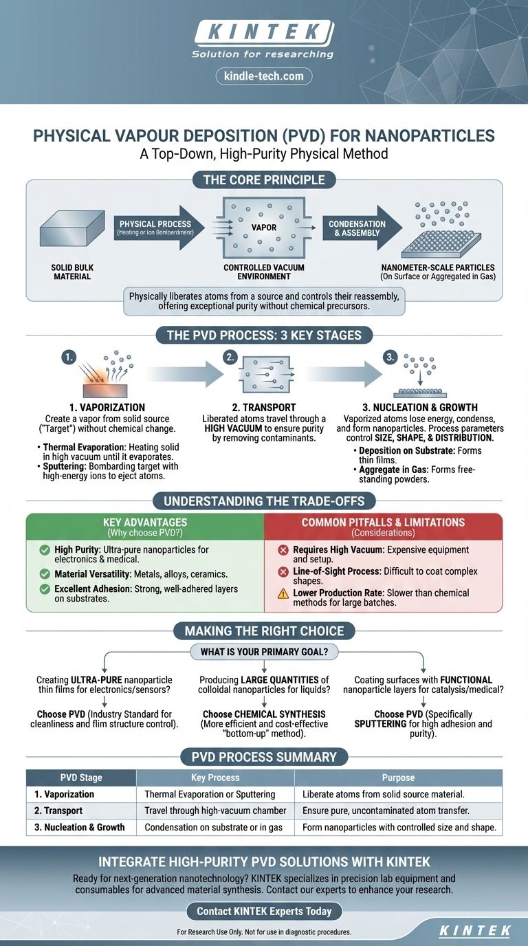
In essence, Physical Vapor Deposition (PVD) for nanoparticles is a "top-down" method where a solid bulk material is converted into a vapor through a physical process, such as heating or ion bombardment. This vapor then travels through a controlled environment—typically a vacuum—and condenses to form nanometer-scale particles, either on a surface or by aggregating in a gas. This technique is fundamentally different from chemical methods, which build nanoparticles from molecular precursors through chemical reactions.
The core principle of PVD is to physically liberate atoms from a source material and then carefully control their reassembly into nanoparticles. This process offers exceptional purity and control, as it avoids the chemical precursors and by-products inherent in other methods.
The PVD Process: From Solid to Nanoparticle
Physical Vapor Deposition is not a single technique but a family of processes. However, they all share three fundamental stages that transform a bulk material into a collection of nanoparticles.
Stage 1: Vaporization
The first step is to create a vapor from a solid source material, known as the "target." This is achieved without chemical change.
The two most common methods are thermal evaporation and sputtering.
- Thermal Evaporation: The source material is heated in a high vacuum until it evaporates or sublimes, much like boiling water turns it into steam.
- Sputtering: The target is bombarded with high-energy ions (usually from an inert gas like argon). This bombardment physically knocks atoms off the target's surface, ejecting them into the vacuum chamber.
Stage 2: Transport
Once atoms are liberated from the source, they travel through the controlled environment.
This transport phase is almost always conducted in a vacuum. The vacuum is critical because it removes other gas molecules that could collide with and contaminate the vaporized atoms, ensuring a pure final product.
Stage 3: Nucleation and Growth
This is the final and most critical stage where nanoparticles are formed.
As the vaporized atoms travel, they lose energy and begin to condense. They can either deposit onto a solid surface (a substrate) to form a thin film of nanoparticles or they can collide with each other in the inert gas to form free-standing nanoparticles, which can then be collected as a powder.
The final size, shape, and distribution of the nanoparticles are precisely controlled by tuning process parameters like pressure, temperature, and deposition time.
Understanding the Trade-offs of PVD
PVD is a powerful technique, but its suitability depends entirely on the application. Understanding its advantages and limitations is key to making an informed decision.
Key Advantages
- High Purity: Because PVD starts with a pure, solid source and avoids chemical reactants, the resulting nanoparticles can be exceptionally pure. This is critical for electronics and medical applications.
- Material Versatility: A vast range of materials, including metals, alloys, and ceramics, can be deposited using PVD.
- Excellent Adhesion: When depositing nanoparticles as a film onto a substrate, PVD methods typically create a very strong, well-adhered layer.
Common Pitfalls and Limitations
- Requires High Vacuum: PVD systems need sophisticated and expensive vacuum equipment, making the initial setup cost high.
- Line-of-Sight Process: In most PVD setups, the source material can only coat surfaces that are in its direct line of sight. This can make it difficult to coat complex, three-dimensional shapes uniformly.
- Lower Production Rate: Compared to large-scale chemical synthesis methods that produce nanoparticles in a liquid batch, PVD can be a slower process, making it less suitable for mass production of nanoparticle powders.
Making the Right Choice for Your Goal
Selecting a synthesis method requires matching the technique's strengths to your primary objective. PVD excels where purity and precise surface deposition are paramount.
- If your primary focus is creating ultra-pure nanoparticle thin films for electronics or sensors: PVD is an industry-standard choice due to its cleanliness and control over film structure.
- If your primary focus is producing large quantities of colloidal nanoparticles for use in liquids or composites: A "bottom-up" chemical synthesis method is almost always more efficient and cost-effective.
- If your primary focus is coating a surface with a functional nanoparticle layer for catalysis or medical implants: PVD, particularly sputtering, provides the high adhesion and purity required for these demanding applications.
Ultimately, PVD is the definitive choice when you need to physically construct a high-purity nanostructured surface or material directly from a solid source.
Summary Table:
| PVD Stage | Key Process | Purpose |
|---|---|---|
| 1. Vaporization | Thermal Evaporation or Sputtering | Liberate atoms from a solid source material. |
| 2. Transport | Travel through a high-vacuum chamber | Ensure pure, uncontaminated atom transfer. |
| 3. Nucleation & Growth | Condensation on a substrate or in gas | Form nanoparticles with controlled size and shape. |
Ready to integrate high-purity PVD nanoparticles into your research or production? KINTEK specializes in precision lab equipment and consumables for advanced material synthesis. Whether you're developing next-generation electronics, medical implants, or catalytic surfaces, our solutions provide the control and purity your laboratory demands. Contact our experts today to discuss how our PVD systems can enhance your nanotechnology projects.
Visual Guide
Related Products
- Chemical Vapor Deposition CVD Equipment System Chamber Slide PECVD Tube Furnace with Liquid Gasifier PECVD Machine
- RF PECVD System Radio Frequency Plasma-Enhanced Chemical Vapor Deposition RF PECVD
- 915MHz MPCVD Diamond Machine Microwave Plasma Chemical Vapor Deposition System Reactor
- HFCVD Machine System Equipment for Drawing Die Nano-Diamond Coating
- Customer Made Versatile CVD Tube Furnace Chemical Vapor Deposition Chamber System Equipment
People Also Ask
- What are the advantages of chemical vapor deposition? Achieve Superior Thin Films for Your Lab
- What happens during deposition chemistry? Building Thin Films from Gaseous Precursors
- How are carbon nanotubes grown? Master Scalable Production with Chemical Vapor Deposition
- What are the processes of vapor phase deposition? Understand CVD vs. PVD for Superior Thin Films
- What types of substrates are used in CVD to facilitate graphene films? Optimize Graphene Growth with the Right Catalyst


