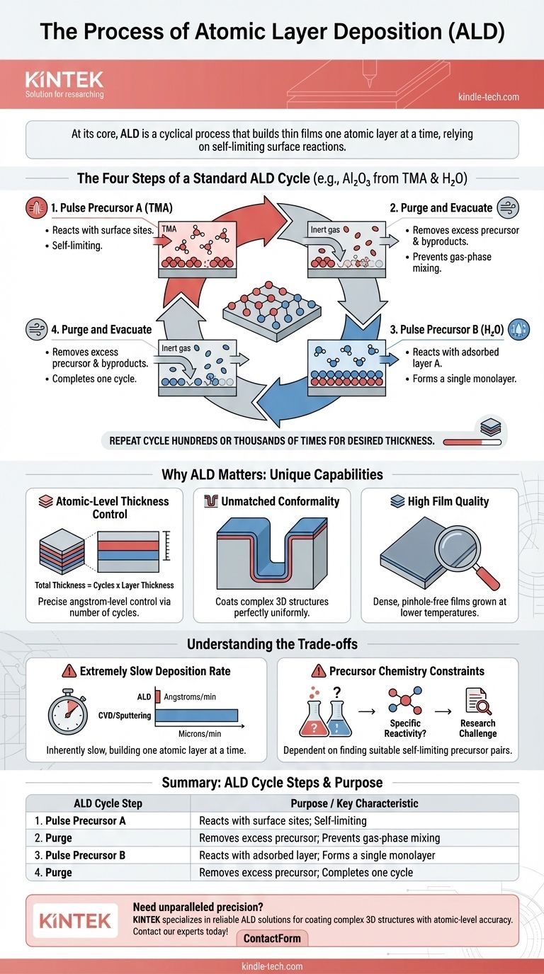
At its core, Atomic Layer Deposition (ALD) is a cyclical process that builds thin films one atomic layer at a time. Unlike other methods that deposit material continuously, ALD relies on a sequence of self-limiting chemical reactions. This fundamental difference gives it unparalleled control over film thickness and the ability to coat highly complex, three-dimensional surfaces with perfect uniformity.
The defining characteristic of ALD is its four-step cycle: expose the surface to a chemical precursor, purge the excess, expose it to a second precursor to react with the first, and purge the excess again. This deliberate, layer-by-layer construction is the key to its precision.
The Four Steps of a Standard ALD Cycle
ALD's power comes from separating the chemical reactions in time. Let's use the common example of depositing aluminum oxide (Al₂O₃) from two chemicals: trimethylaluminum (TMA) as the aluminum precursor and water (H₂O) as the oxygen precursor.
Step 1: Pulse Precursor A (TMA)
The first chemical precursor, TMA, is introduced into the reaction chamber as a gas.
The TMA molecules react with the available bonding sites on the substrate surface until every site is occupied. This process is self-limiting; once the surface is saturated, no more TMA can attach.
Step 2: Purge and Evacuate
Any excess TMA molecules that did not react, along with any gaseous byproducts, are removed from the chamber.
This is typically done by flushing the chamber with an inert gas, like nitrogen or argon. This purge step is critical to prevent the precursors from mixing in the gas phase, which would cause uncontrolled deposition.
Step 3: Pulse Precursor B (H₂O)
The second chemical precursor, in this case water vapor, is pulsed into the chamber.
These water molecules react exclusively with the TMA molecules that are already bound to the surface. This reaction forms a uniform, single layer of aluminum oxide (Al₂O₃) and prepares the surface with new reactive sites for the next cycle.
Step 4: Purge and Evacuate
The chamber is purged with inert gas again to remove any unreacted water vapor and gaseous byproducts from the second reaction.
This completes one full ALD cycle, having deposited a single, precise monolayer of the target material. The entire four-step process is then repeated hundreds or thousands of times to achieve the desired film thickness.
Why This Cyclical Process Matters
The unique, sequential nature of ALD provides capabilities that are difficult or impossible to achieve with other deposition techniques like sputtering or chemical vapor deposition (CVD).
Atomic-Level Thickness Control
Since each cycle adds a predictable amount of material (typically a fraction of a monolayer), the final film thickness is determined simply by the number of cycles performed. This allows for angstrom-level precision.
Unmatched Conformality
Because the gaseous precursors can reach any part of the substrate, ALD can deposit a perfectly uniform film over incredibly complex and high-aspect-ratio structures. The film thickness will be the same at the top, bottom, and sidewalls of a deep trench.
High Film Quality
ALD can often be performed at lower temperatures than other methods. The self-limiting nature of the reactions ensures the growth of dense, pinhole-free films with low impurity levels.
Understanding the Trade-offs
Despite its powerful advantages, ALD is not the solution for every application. Its primary limitation is a direct consequence of its layer-by-layer nature.
Extremely Slow Deposition Rate
Building a film one atomic layer at a time is inherently slow. ALD growth rates are typically measured in angstroms or nanometers per minute, which is orders of magnitude slower than sputtering or CVD.
Precursor Chemistry Constraints
The process is entirely dependent on finding pairs of precursor chemicals that have the correct self-limiting reactivity. Developing a new ALD process for a novel material can be a significant research and development challenge.
Making the Right Choice for Your Goal
Selecting a deposition method requires aligning the process capabilities with your primary objective.
- If your primary focus is ultimate precision and coating complex 3D structures: ALD is the unmatched choice for applications like advanced microelectronics, MEMS, and catalysis.
- If your primary focus is depositing a thick film quickly and cost-effectively: A different method like sputtering or physical vapor deposition (PVD) is almost always more suitable.
- If your primary focus is high-quality films on simple, flat surfaces: Both ALD and Plasma-Enhanced Chemical Vapor Deposition (PECVD) could be viable options, with the choice often depending on speed and specific film property requirements.
Ultimately, choosing ALD is a commitment to precision and perfection over speed.
Summary Table:
| ALD Cycle Step | Purpose | Key Characteristic |
|---|---|---|
| 1. Pulse Precursor A | Reacts with surface sites | Self-limiting reaction |
| 2. Purge | Removes excess precursor A | Prevents gas-phase mixing |
| 3. Pulse Precursor B | Reacts with adsorbed layer A | Forms a single monolayer |
| 4. Purge | Removes excess precursor B | Completes one cycle |
Need unparalleled precision for your thin-film applications? KINTEK specializes in lab equipment and consumables, providing the reliable ALD solutions your laboratory requires for coating complex 3D structures with atomic-level accuracy. Contact our experts today to discuss how our ALD systems can enhance your research and development!
Visual Guide
Related Products
- Aluminized Ceramic Evaporation Boat for Thin Film Deposition
- Chemical Vapor Deposition CVD Equipment System Chamber Slide PECVD Tube Furnace with Liquid Gasifier PECVD Machine
- HFCVD Machine System Equipment for Drawing Die Nano-Diamond Coating
- RF PECVD System Radio Frequency Plasma-Enhanced Chemical Vapor Deposition RF PECVD
- Customer Made Versatile CVD Tube Furnace Chemical Vapor Deposition Chamber System Equipment
People Also Ask
- What are the alternatives to sputtering? Choose the Right Thin Film Deposition Method
- What is the source of evaporation for thin film? Choosing Between Thermal and E-Beam Methods
- Why are high-purity ceramic boats used for lignin activation? Ensure Purity & Thermal Stability
- What is the chemical method for thin film deposition? Build Films from the Molecular Level Up
- Why is an alumina boat selected for catalyst precursors? Ensure Sample Purity at 1000 °C


