At its core, the production of graphene via Chemical Vapor Deposition (CVD) is a high-temperature coating process. It involves flowing a hydrocarbon gas over a heated metal substrate in a reaction chamber, causing the gas to decompose and allowing the resulting carbon atoms to assemble into a single, continuous atomic layer of graphene on the metal's surface.
Chemical Vapor Deposition is fundamentally a "bottom-up" assembly technique. It uses high heat to break down a simple carbon source and a catalytic metal surface to guide those free carbon atoms into forming large, high-quality sheets of graphene, making it the only viable method for industrial-scale production.
Deconstructing the CVD Process
The CVD method can be understood as a carefully orchestrated, multi-step procedure that transforms a simple gas into a highly structured, two-dimensional material. Each stage requires precise environmental control.
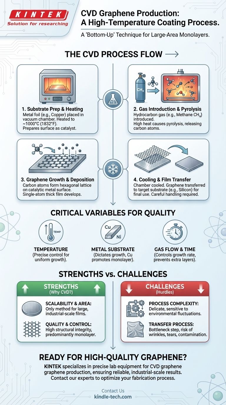
Step 1: Substrate Preparation and Heating
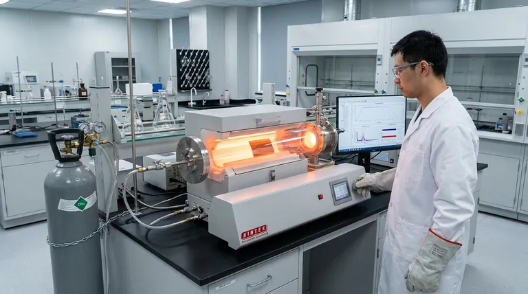
The process begins by placing a metal substrate, typically a thin foil of copper (Cu) or nickel (Ni), inside a vacuum furnace or reaction chamber. This chamber is then heated to extremely high temperatures, usually around 1000°C (1832°F). This intense heat prepares the metal surface to act as a catalyst.
Step 2: Gas Introduction and Pyrolysis
Once the substrate reaches the target temperature, a carbon-containing precursor gas is introduced into the chamber. Methane (CH₄) is a common and effective choice for this precursor. The high temperature causes the gas molecules to break apart in a process called pyrolysis, releasing individual carbon atoms.
Step 3: Graphene Growth and Deposition
These newly freed carbon atoms move across the hot metal surface. The metal acts as a catalytic substrate, guiding the carbon atoms to arrange themselves into the stable, hexagonal lattice structure characteristic of graphene. This process continues until a continuous, single-atom-thick film covers the substrate.
Step 4: Cooling and Film Transfer
After the growth is complete, the chamber is cooled down. The graphene film, now resting on the metal foil, is not yet in its final usable form. It must be carefully transferred from the growth substrate to a target substrate (like silicon or PET) for use in electronic devices or other applications.
Key Variables That Define the Outcome
The quality, thickness, and uniformity of the final graphene sheet are not accidental. They are the direct result of manipulating several critical parameters during the growth process.
The Role of Temperature
Temperature is arguably the most critical variable. It must be high enough to efficiently decompose the hydrocarbon gas but controlled precisely to ensure uniform growth. Deviations can lead to defects or the formation of multiple, undesirable layers of graphene.
The Function of the Metal Substrate
The choice of metal substrate is crucial as it dictates the growth mechanism. Copper is widely used because it has low carbon solubility, which naturally promotes the formation of a single layer (monolayer) of graphene.
The Impact of Gas Flow and Time
The rate at which the hydrocarbon gas is introduced and the total duration of the exposure directly influence the final product. These parameters are carefully tuned to control the growth rate and ensure complete, uniform coverage without creating unwanted extra layers.
Understanding the Trade-offs
While CVD is the leading method for large-scale graphene production, it is essential to understand its strengths and inherent challenges.
Strength: Scalability and Area
CVD is the only proven method capable of producing large-area graphene sheets on an industrial scale. This makes it indispensable for applications in electronics, transparent conductors, and sensors that require uniform, wafer-scale films.
Strength: Quality and Control
The process allows for a high degree of control, enabling the synthesis of high-quality, predominantly monolayer graphene. This level of structural integrity is critical for leveraging graphene's exceptional electronic properties.
Challenge: Process Complexity
The method is delicate and highly sensitive to fluctuations in temperature, pressure, and gas flow. Achieving consistent, high-quality results requires sophisticated equipment and meticulous process control.
Challenge: The Transfer Process
A significant bottleneck is the post-growth transfer step. Moving the atomically thin graphene sheet from the metal foil to a target substrate is a complex procedure that can easily introduce wrinkles, tears, and contamination, potentially degrading the material's performance.
Making the Right Choice for Your Goal
Understanding the CVD process allows you to align the method with your specific objective.
- If your primary focus is creating large-area films for electronics: CVD is the definitive industrial standard due to its unmatched ability to produce uniform, high-quality monolayer sheets.
- If your primary focus is developing bulk material composites or inks: You should explore alternative methods like liquid-phase exfoliation, as the film-based nature of CVD is not suited for creating powders or dispersions.
- If your primary focus is fundamental research: Mastering CVD's control variables is paramount for tuning graphene's electronic and physical properties to meet specific experimental demands.
Mastering the principles of chemical vapor deposition is fundamental to harnessing the full potential of graphene at a meaningful scale.
Summary Table:
| CVD Process Step | Key Action | Typical Parameters |
|---|---|---|
| 1. Substrate Prep & Heating | Metal foil (e.g., Cu) is heated in a vacuum chamber | ~1000°C (1832°F) |
| 2. Gas Introduction & Pyrolysis | Hydrocarbon gas (e.g., methane) is flowed into the chamber | Gas decomposes (pyrolysis) |
| 3. Graphene Growth & Deposition | Carbon atoms form a hexagonal lattice on the catalytic metal surface | Guided by metal substrate |
| 4. Cooling & Film Transfer | Graphene is transferred to a target substrate (e.g., silicon) | Requires careful handling to avoid defects |
Ready to integrate high-quality graphene into your research or product development? KINTEK specializes in providing the precise lab equipment and consumables needed for advanced materials synthesis like CVD graphene production. Our expertise ensures you have the reliable tools and support to achieve consistent, industrial-scale results. Contact our experts today to discuss how we can optimize your graphene fabrication process.
Visual Guide
Related Products
- HFCVD Machine System Equipment for Drawing Die Nano-Diamond Coating
- Customer Made Versatile CVD Tube Furnace Chemical Vapor Deposition Chamber System Equipment
- Chemical Vapor Deposition CVD Equipment System Chamber Slide PECVD Tube Furnace with Liquid Gasifier PECVD Machine
- Multi Heating Zones CVD Tube Furnace Machine Chemical Vapor Deposition Chamber System Equipment
- Microwave Plasma Chemical Vapor Deposition MPCVD Machine System Reactor for Lab and Diamond Growth
People Also Ask
- What is the specific function of the metal filament in HF-CVD? Key Roles in Diamond Growth
- What is the full form of HFCVD? A Guide to Hot Filament Chemical Vapor Deposition
- What are the disadvantages and challenges of the HFCVD method? Overcome Growth Limits and Filament Issues
- What is the chemical vapor deposition growth process? Build Superior Thin Films from the Atom Up
- What are the advantages of chemical vapor deposition? Achieve Superior Thin Films for Your Lab


