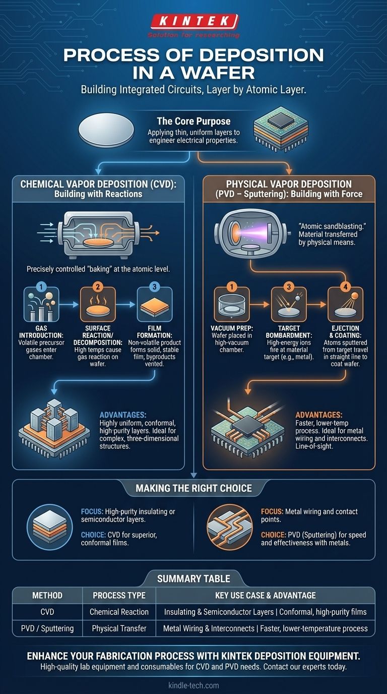
In short, wafer deposition is the process of applying thin, uniform layers of material onto a silicon wafer to build the components of an integrated circuit. The two primary methods are Chemical Vapor Deposition (CVD), where precursor gases react on the wafer's surface to form a solid film, and Physical Vapor Deposition (PVD), like sputtering, where a material is physically blasted from a target and transferred onto the wafer.
The core purpose of deposition is not simply to add material, but to precisely engineer the electrical properties of a chip, layer by atomic layer. The choice of method depends entirely on the material being deposited and the structural requirements of the final device.
The Two Pillars of Deposition: Physical vs. Chemical
At its heart, all wafer deposition falls into two categories. Understanding this distinction is key to understanding the entire process.
Chemical Vapor Deposition (CVD): Building with Reactions
CVD is a process where a wafer (the substrate) is exposed to one or more volatile precursor gases. These gases react or decompose on the substrate's surface to produce the desired solid film.
Think of it as precisely controlled "baking" at the atomic level.
The process involves three fundamental stages:
- A volatile compound of the material you want to deposit is introduced into a reaction chamber as a gas.
- High temperatures cause this gas to either decompose or react with other gases right at the wafer's surface.
- The non-volatile product of that reaction forms a solid, stable film on the substrate, with other byproducts being vented away.
CVD is exceptional for creating highly uniform, pure, and conformal layers, meaning it can evenly coat complex, three-dimensional structures on a chip.
Physical Vapor Deposition (PVD): Building with Force
PVD methods transfer a material from a source to the substrate through purely physical means, typically in a high-vacuum environment. The most common PVD technique in semiconductor manufacturing is sputtering.
Sputtering is best understood as "atomic sandblasting."
The operational procedure for sputtering typically involves these steps:
- A high-vacuum chamber is prepared, and the wafer is placed inside.
- The substrate is often cleaned with an ion etch to remove any surface contaminants, ensuring good adhesion.
- High-energy ions are fired at a target made of the material you want to deposit (e.g., aluminum or copper).
- This bombardment ejects or "sputters" atoms from the target, which then travel in a straight line and coat the wafer.
PVD is a line-of-sight process, which makes it ideal for depositing metals but less effective at coating the vertical sidewalls of deep trenches.
Understanding the Trade-offs
Neither method is universally superior; they are tools selected for specific jobs based on their inherent advantages and disadvantages.
When to Use CVD
CVD is the preferred method when layer quality and conformity are paramount. It is the workhorse for creating insulating layers (like silicon dioxide) and semiconductor films (like polysilicon) because the chemical reaction can build perfect atomic structures.
However, CVD often requires very high temperatures, which can damage previously fabricated structures on the wafer. The chemical precursors can also be highly toxic and expensive.
When to Use PVD (Sputtering)
Sputtering excels at depositing metals and other alloys for the chip's wiring, known as interconnects. It is a faster and generally lower-temperature process than CVD.
The primary drawback of sputtering is its poor step coverage. Because the sputtered atoms travel in straight lines, they tend to build up on horizontal surfaces but thinly coat vertical ones, which can be a problem for increasingly complex chip architectures.
Making the Right Choice for Your Goal
The decision between CVD and PVD is dictated by the specific layer being built and its role in the final integrated circuit.
- If your primary focus is creating high-purity insulating or semiconductor layers: Your choice is almost always a form of CVD for its ability to produce superior, conformal films.
- If your primary focus is depositing the metal wiring and contact points: PVD, specifically sputtering, is the industry standard due to its speed and effectiveness with metallic materials.
Ultimately, deposition transforms a blank silicon canvas into a multi-layered electronic marvel, with each method playing a critical and distinct role in the fabrication process.
Summary Table:
| Method | Process Type | Key Use Case | Key Advantage |
|---|---|---|---|
| Chemical Vapor Deposition (CVD) | Chemical Reaction | Insulating & Semiconductor Layers | Conformal, high-purity films |
| Physical Vapor Deposition (PVD / Sputtering) | Physical Transfer | Metal Wiring & Interconnects | Faster, lower-temperature process |
Ready to enhance your semiconductor fabrication process with precision deposition equipment? KINTEK specializes in high-quality lab equipment and consumables for all your wafer processing needs. Whether you require the superior conformity of CVD systems or the efficient metal deposition of PVD sputtering tools, our solutions are designed to meet the exacting standards of modern laboratories. Contact our experts today to discuss how we can support your specific application and help you achieve flawless results.
Visual Guide
Related Products
- HFCVD Machine System Equipment for Drawing Die Nano-Diamond Coating
- 915MHz MPCVD Diamond Machine Microwave Plasma Chemical Vapor Deposition System Reactor
- Chemical Vapor Deposition CVD Equipment System Chamber Slide PECVD Tube Furnace with Liquid Gasifier PECVD Machine
- Cylindrical Resonator MPCVD Machine System Reactor for Microwave Plasma Chemical Vapor Deposition and Lab Diamond Growth
- Microwave Plasma Chemical Vapor Deposition MPCVD Machine System Reactor for Lab and Diamond Growth
People Also Ask
- What are the advantages of chemical vapor deposition? Achieve Superior Thin Films for Your Lab
- How expensive is chemical vapor deposition? Understanding the True Cost of High-Performance Coating
- What are the disadvantages and challenges of the HFCVD method? Overcome Growth Limits and Filament Issues
- What types of substrates are used in CVD to facilitate graphene films? Optimize Graphene Growth with the Right Catalyst
- What is the function of tungsten filaments in HFCVD? Powering Diamond Film Synthesis with Thermal Excitation