Knowledge What is the process of deposition in semiconductors? Build Precise Thin Films for Your ICs
Author avatar

Tech Team · Kintek Solution

Updated 2 weeks ago

What is the process of deposition in semiconductors? Build Precise Thin Films for Your ICs

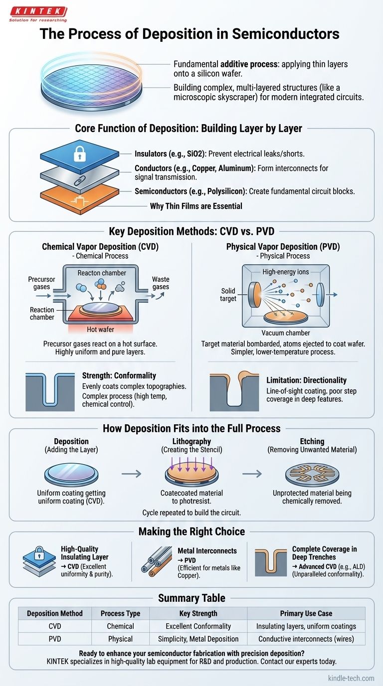
In semiconductor manufacturing, deposition is the fundamental process of applying thin layers of material onto a silicon wafer. This is a purely additive process, where materials like insulators, conductors, or semiconductors are grown or coated onto the wafer's surface, often just a few atomic layers at a time. It is the primary method for building the intricate, multi-layered structures that form modern integrated circuits.

The critical concept to understand is that deposition is about adding a uniform layer of material to a wafer. This is distinct from photolithography (patterning the layer) and etching (selectively removing parts of the layer), which are separate, subsequent steps in the fabrication sequence.

The Core Function of Deposition

Building the Circuit, Layer by Layer

Think of a microprocessor as a microscopic, multi-story skyscraper. Deposition is the process of adding each new floor (an insulating layer) or the wiring within the walls (a conductive layer).

This process is repeated hundreds of times to build the complex vertical structure of a modern chip. The quality and precision of each deposited layer are paramount to the final device's performance.

Why Thin Films are Essential

The thin films created by deposition serve specific, critical functions:

  • Insulators (e.g., silicon dioxide, silicon nitride) prevent electrical currents from leaking or shorting out between different components.
  • Conductors (e.g., copper, aluminum, tungsten) form the microscopic wires, or "interconnects," that transmit signals between transistors.
  • Semiconductors (e.g., polysilicon) are used to create the fundamental building blocks of the circuit, such as the transistor gates.

Key Deposition Methods: CVD vs. PVD

While there are many specific techniques, nearly all deposition processes fall into two main families: Chemical Vapor Deposition (CVD) and Physical Vapor Deposition (PVD).

Chemical Vapor Deposition (CVD)

CVD is a chemical process. Precursor gases are introduced into a reaction chamber containing the heated wafer.

These gases react on the hot surface, leaving behind a solid thin film of the desired material and releasing other gaseous byproducts, which are then vented. This method is known for producing highly uniform and pure layers.

Physical Vapor Deposition (PVD)

PVD is a physical process, often compared to atomic-level spray painting. Inside a vacuum chamber, a solid source material (called a "target") is bombarded with high-energy ions.

This bombardment knocks atoms loose from the target. These atoms then travel through the vacuum and coat the wafer, building up the thin film atom by atom.

Understanding the Trade-offs

The choice between CVD and PVD is dictated by the material being deposited and the structural requirements of the layer.

CVD: Conformality vs. Complexity

CVD's strength is its conformality. Because the chemical reaction happens everywhere on the surface, it can evenly coat the bottom and sides of very deep, narrow trenches in the wafer's topography.

The trade-off is complexity. CVD often requires high temperatures and involves volatile chemical reactions that must be precisely controlled to ensure layer purity and prevent defects.

PVD: Simplicity vs. Directionality

PVD is often a simpler, lower-temperature process, which is ideal for depositing metals that can't withstand the high heat of CVD.

Its primary limitation is directionality. Because the atoms travel in a "line-of-sight" from the target to the wafer, PVD can struggle to evenly coat the sidewalls of deep features, a problem known as poor "step coverage."

How Deposition Fits into the Full Process

The steps described in some manufacturing guides can be confusing. Deposition is only the first part of a three-step cycle that is repeated over and over.

Step 1: Deposition (Adding the Layer)

A uniform layer of material, such as silicon nitride, is deposited across the entire surface of the wafer using a method like CVD.

Step 2: Lithography (Creating the Stencil)

A light-sensitive material called photoresist is coated on top of the deposited layer. It is then exposed to UV light through a patterned mask, and the pattern is developed, creating a protective stencil.

Step 3: Etching (Removing Unwanted Material)

A chemical or plasma etching process removes the silicon nitride in the areas not protected by the photoresist stencil. Finally, the remaining photoresist is stripped away, leaving behind the desired circuit pattern.

Making the Right Choice for Your Goal

The choice between deposition methods is dictated entirely by the specific layer's function within the integrated circuit.

  • If your primary focus is creating a high-quality insulating layer (e.g., a transistor gate oxide): Chemical Vapor Deposition (CVD) is the preferred method for its excellent uniformity and purity.
  • If your primary focus is creating the metal interconnects (wires): Physical Vapor Deposition (PVD) is commonly used for its efficiency in depositing metals like copper or aluminum.
  • If your primary focus is ensuring complete coverage in deep, narrow trenches: Advanced techniques like Atomic Layer Deposition (ALD), a precise sub-type of CVD, are required for their unparalleled conformality.

Ultimately, mastering deposition is about selecting the right additive technique to precisely build the foundation for each subsequent patterning and etching step.

Summary Table:

Deposition Method Process Type Key Strength Primary Use Case
Chemical Vapor Deposition (CVD) Chemical Excellent Conformality Insulating layers, uniform coatings
Physical Vapor Deposition (PVD) Physical Simplicity, Metal Deposition Conductive interconnects (wires)

Ready to enhance your semiconductor fabrication process with precision deposition? KINTEK specializes in high-quality lab equipment and consumables for semiconductor R&D and production. Whether you require CVD systems for uniform insulating layers or PVD tools for reliable metal interconnects, our solutions are designed to meet the stringent demands of modern chip manufacturing. Contact our experts today to discuss how we can support your laboratory's specific deposition needs and help you build better integrated circuits.

Related Products

People Also Ask

Related Products

Inclined Rotary Plasma Enhanced Chemical Vapor Deposition PECVD Equipment Tube Furnace Machine

Inclined Rotary Plasma Enhanced Chemical Vapor Deposition PECVD Equipment Tube Furnace Machine

Upgrade your coating process with PECVD coating equipment. Ideal for LED, power semiconductors, MEMS and more. Deposits high-quality solid films at low temps.

HFCVD Machine System Equipment for Drawing Die Nano-Diamond Coating

HFCVD Machine System Equipment for Drawing Die Nano-Diamond Coating

The nano-diamond composite coating drawing die uses cemented carbide (WC-Co) as the substrate, and uses the chemical vapor phase method ( CVD method for short ) to coat the conventional diamond and nano-diamond composite coating on the surface of the inner hole of the mold.

Vacuum Hot Press Furnace Machine for Lamination and Heating

Vacuum Hot Press Furnace Machine for Lamination and Heating

Experience clean and precise lamination with Vacuum Lamination Press. Perfect for wafer bonding, thin-film transformations, and LCP lamination. Order now!

915MHz MPCVD Diamond Machine Microwave Plasma Chemical Vapor Deposition System Reactor

915MHz MPCVD Diamond Machine Microwave Plasma Chemical Vapor Deposition System Reactor

915MHz MPCVD Diamond Machine and its multi-crystal effective growth, the maximum area can reach 8 inches, the maximum effective growth area of single crystal can reach 5 inches. This equipment is mainly used for the production of large-size polycrystalline diamond films, the growth of long single crystal diamonds, the low-temperature growth of high-quality graphene, and other materials that require energy provided by microwave plasma for growth.

Laboratory CVD Boron Doped Diamond Materials

Laboratory CVD Boron Doped Diamond Materials

CVD boron-doped diamond: A versatile material enabling tailored electrical conductivity, optical transparency, and exceptional thermal properties for applications in electronics, optics, sensing, and quantum technologies.

Laboratory Quartz Tube Furnace Tubular RTP Heating Furnace

Laboratory Quartz Tube Furnace Tubular RTP Heating Furnace

Get lightning-fast heating with our RTP Rapid Heating Tube Furnace. Designed for precise, high-speed heating and cooling with convenient sliding rail and TFT touch screen controller. Order now for ideal thermal processing!

1400℃ Laboratory Quartz Tube Furnace with Alumina Tube Tubular Furnace

1400℃ Laboratory Quartz Tube Furnace with Alumina Tube Tubular Furnace

Looking for a tube furnace for high-temperature applications? Our 1400℃ Tube Furnace with Alumina Tube is perfect for research and industrial use.

Small Vacuum Heat Treat and Tungsten Wire Sintering Furnace

Small Vacuum Heat Treat and Tungsten Wire Sintering Furnace

The small vacuum tungsten wire sintering furnace is a compact experimental vacuum furnace specially designed for universities and scientific research institutes. The furnace features a CNC welded shell and vacuum piping to ensure leak-free operation. Quick-connect electrical connections facilitate relocation and debugging, and the standard electrical control cabinet is safe and convenient to operate.

Graphite Vacuum Furnace High Thermal Conductivity Film Graphitization Furnace

Graphite Vacuum Furnace High Thermal Conductivity Film Graphitization Furnace

The high thermal conductivity film graphitization furnace has uniform temperature, low energy consumption and can operate continuously.

Vacuum Heat Treat and Molybdenum Wire Sintering Furnace for Vacuum Sintering

Vacuum Heat Treat and Molybdenum Wire Sintering Furnace for Vacuum Sintering

A vacuum molybdenum wire sintering furnace is a vertical or bedroom structure, which is suitable for withdrawal, brazing, sintering and degassing of metal materials under high vacuum and high temperature conditions. It is also suitable for dehydroxylation treatment of quartz materials.

High Temperature Muffle Oven Furnace for Laboratory Debinding and Pre Sintering

High Temperature Muffle Oven Furnace for Laboratory Debinding and Pre Sintering

KT-MD High temperature debinding and pre-sintering furnace for ceramic materials with various molding processes. Ideal for electronic components such as MLCC and NFC.

Molybdenum Vacuum Heat Treat Furnace

Molybdenum Vacuum Heat Treat Furnace

Discover the benefits of a high-configuration molybdenum vacuum furnace with heat shield insulation. Ideal for high-purity, vacuum environments like sapphire crystal growth and heat treatment.

Graphite Vacuum Furnace IGBT Experimental Graphitization Furnace

Graphite Vacuum Furnace IGBT Experimental Graphitization Furnace

IGBT experimental graphitization furnace, a tailored solution for universities and research institutions, with high heating efficiency, user-friendliness, and precise temperature control.

Laboratory Vacuum Tilt Rotary Tube Furnace Rotating Tube Furnace

Laboratory Vacuum Tilt Rotary Tube Furnace Rotating Tube Furnace

Discover the versatility of Laboratory Rotary Furnace: Ideal for calcination, drying, sintering, and high-temperature reactions. Adjustable rotating and tilting functions for optimal heating. Suitable for vacuum and controlled atmosphere environments. Learn more now!

Vacuum Dental Porcelain Sintering Furnace

Vacuum Dental Porcelain Sintering Furnace

Get precise and reliable results with KinTek's Vacuum Porcelain Furnace. Suitable for all porcelain powders, it features hyperbolic ceramic furnace function, voice prompt, and automatic temperature calibration.

Vacuum Sealed Continuous Working Rotary Tube Furnace Rotating Tube Furnace

Vacuum Sealed Continuous Working Rotary Tube Furnace Rotating Tube Furnace

Experience efficient material processing with our vacuum-sealed rotary tube furnace. Perfect for experiments or industrial production, equipped with optional features for controlled feeding and optimized results. Order now.

1700℃ Muffle Oven Furnace for Laboratory

1700℃ Muffle Oven Furnace for Laboratory

Get superior heat control with our 1700℃ Muffle Furnace. Equipped with intelligent temperature microprocessor, TFT touch screen controller & advanced insulation materials for precise heating up to 1700C. Order now!

Laboratory Sterilizer Lab Autoclave Vertical Pressure Steam Sterilizer for Liquid Crystal Display Automatic Type

Laboratory Sterilizer Lab Autoclave Vertical Pressure Steam Sterilizer for Liquid Crystal Display Automatic Type

Liquid crystal display automatic vertical sterilizer is a safe, reliable and automatic control sterilization equipment, which is composed of heating system, microcomputer control system and overheating and overvoltage protection system.

Laboratory Sterilizer Lab Autoclave Pulse Vacuum Lifting Sterilizer

Laboratory Sterilizer Lab Autoclave Pulse Vacuum Lifting Sterilizer

The pulse vacuum lifting sterilizer is a state-of-the-art equipment for efficient and precise sterilization. It uses pulsating vacuum technology, customizable cycles, and a user-friendly design for easy operation and safety.

Anti-Cracking Press Mold for Lab Use

Anti-Cracking Press Mold for Lab Use

The anti-cracking press mold is a specialized equipment designed for molding various shapes and sizes of film using high pressure and electric heating.


Leave Your Message