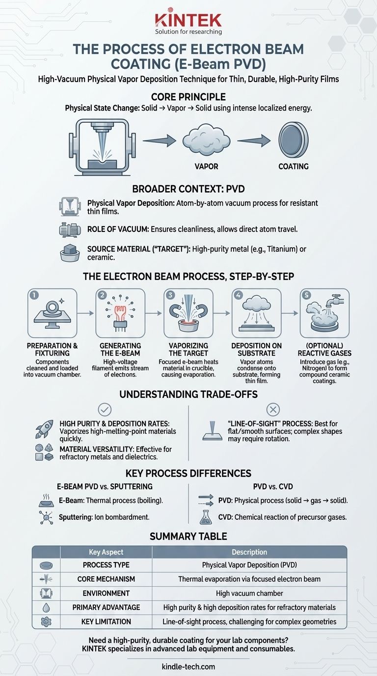
In essence, electron beam coating is a high-vacuum process where a powerful, focused beam of electrons is used to boil a solid source material, turning it directly into a vapor. This vapor then travels through the vacuum and condenses onto the surface of a target object, forming an extremely thin, durable, and high-purity film. It is a specific and widely used method within a broader category of techniques known as Physical Vapor Deposition (PVD).
The core principle is not a chemical reaction, but a physical state change. An electron beam provides the intense, localized energy needed to transform a solid material into a gas within a vacuum, which then resolidifies atom-by-atom as a precise coating on a component's surface.
Understanding the Broader Context: PVD
To fully grasp electron beam coating, you must first understand its parent technology, Physical Vapor Deposition (PVD). This process forms the foundation for how the coating is applied.
What is Physical Vapor Deposition (PVD)?
PVD refers to a set of vacuum deposition methods used to produce thin films and coatings. In any PVD process, a solid material is vaporized in a vacuum chamber and then deposited onto a substrate.
The deposition occurs on an atom-by-atom basis, creating a thin, bonded layer that is highly resistant to wear and nearly impossible to remove once applied.
The Role of the Vacuum
The entire PVD process takes place under a high vacuum. This is critical for two reasons: it ensures the chamber is exceptionally clean, preventing contamination, and it allows the vaporized atoms to travel directly to the substrate without colliding with air molecules.
The Source Material, or "Target"
The solid material being vaporized is often referred to as the "target" or source material. This can be a high-purity metal like titanium or chromium, or various ceramic compounds. The electron beam is simply one of several methods used to vaporize this target.
The Electron Beam Process, Step-by-Step
While part of a larger workflow that includes cleaning, pre-treatment, and quality control, the core electron beam evaporation stage involves a few precise steps.
Step 1: Preparation and Fixturing
The components to be coated (the substrates) are meticulously cleaned and dried. They are then loaded into the vacuum chamber on specialized fixtures designed to expose the target surfaces to the vapor stream.
Step 2: Generating the Electron Beam
Inside the chamber, a high-voltage system heats a filament, which emits a stream of electrons. This is similar in principle to the electron gun in an old CRT television.
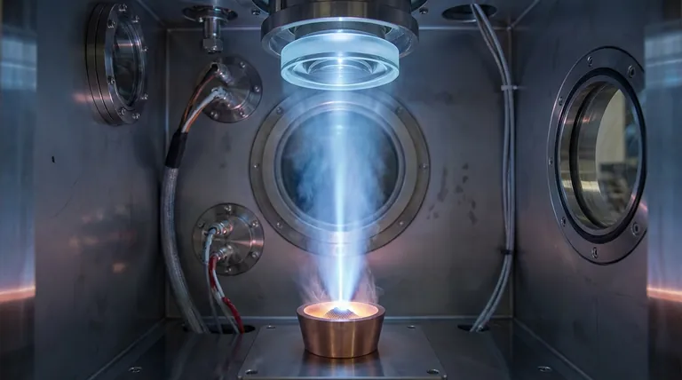
Step 3: Vaporizing the Target Material
Powerful magnetic fields are used to aim and focus this high-energy beam of electrons onto the source material, which is held in a container called a crucible. The intense kinetic energy of the electrons is instantly converted to thermal energy, rapidly heating the material past its boiling point and causing it to evaporate.
Step 4: Deposition on the Substrate
The resulting vapor cloud expands from the crucible and travels in a straight line through the vacuum. When the vapor atoms strike the cooler surface of the substrate, they condense, forming a thin, uniform, and tightly bonded solid film.
Step 5: Creating Compounds with Reactive Gases (Optional)
To create even harder ceramic coatings, a reactive gas like nitrogen or oxygen can be introduced into the chamber during deposition. The vaporized metal atoms react with the gas to form a compound (e.g., titanium nitride), which then deposits on the substrate.
Understanding the Trade-offs
Electron beam PVD is a powerful technique, but it is not universally applicable. Understanding its specific advantages and limitations is key to using it effectively.
Advantage: High Purity and Deposition Rates
The electron beam can generate immense, localized heat. This allows it to vaporize materials with very high melting points and to do so very quickly, resulting in high deposition rates and coatings with exceptional purity.
Advantage: Material Versatility
This method is effective for a vast range of materials, including refractory metals and dielectric compounds that are difficult to vaporize using other PVD techniques like simple thermal evaporation.
Limitation: It's a "Line-of-Sight" Process
Because the vapor travels in a straight line from the source to the substrate, this method is best suited for coating flat or smoothly curved surfaces. Complex shapes with deep recesses or hidden areas may not receive a uniform coating without complex part rotation.
How It Differs from Other Methods
It is critical to distinguish electron beam PVD from other common processes.
E-Beam PVD vs. Sputtering
Sputtering, another PVD method, uses ion bombardment to physically knock atoms off the target material. In contrast, electron beam PVD is a thermal process that uses heat to boil the material.
PVD vs. Chemical Vapor Deposition (CVD)
PVD is a physical process (solid → gas → solid). CVD involves introducing precursor gases into a chamber where they undergo a chemical reaction on the substrate's surface, leaving behind a solid film. The core mechanism is fundamentally different.
Making the Right Choice for Your Goal
Selecting a coating process requires a clear understanding of the desired outcome.
- If your primary focus is high purity and speed for metals or ceramics: Electron beam PVD is an excellent and highly efficient choice, particularly for materials with high melting points.
- If you need to coat complex, non-line-of-sight geometries: You should evaluate whether part rotation is sufficient or if an alternative like sputtering or a CVD process would be more effective.
- If your goal is an exceptionally tough, wear-resistant surface: Combining electron beam PVD with a reactive gas to form a nitride or oxide ceramic coating is a standard and highly effective industry practice.
Ultimately, understanding the mechanism of electron beam coating empowers you to select the precise manufacturing process that meets your material performance requirements.
Summary Table:
| Key Aspect | Description |
|---|---|
| Process Type | Physical Vapor Deposition (PVD) |
| Core Mechanism | Thermal evaporation via focused electron beam |
| Environment | High vacuum chamber |
| Primary Advantage | High purity & high deposition rates for refractory materials |
| Key Limitation | Line-of-sight process, challenging for complex geometries |
Need a high-purity, durable coating for your lab components? KINTEK specializes in advanced lab equipment and consumables for precise coating applications. Our expertise in PVD technologies can help you achieve superior material performance. Contact our experts today to discuss how our solutions can meet your specific laboratory needs.
Visual Guide
Related Products
- Electron Beam Evaporation Coating Conductive Boron Nitride Crucible BN Crucible
- Electron Beam Evaporation Coating Gold Plating Tungsten Molybdenum Crucible for Evaporation
- Electron Beam Evaporation Coating Oxygen-Free Copper Crucible and Evaporation Boat
- E Beam Crucibles Electron Gun Beam Crucible for Evaporation
- HFCVD Machine System Equipment for Drawing Die Nano-Diamond Coating
People Also Ask
- What are the applications of e-beam evaporation? Achieve High-Purity Coatings for Optics & Electronics
- What materials are used in electron beam evaporation? Master High-Purity Thin Film Deposition
- How is an electron beam evaporator cooled during deposition? Essential Thermal Management for Stable Processes
- What is the container that holds the metal source material called in e-beam evaporation? Ensure Purity and Quality in Your Thin-Film Deposition
- Why is Boron Nitride coating used in VHP sintering? Prevent Carbon Diffusion & Ensure Clean Mold Release


