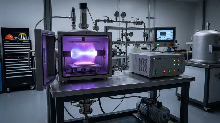
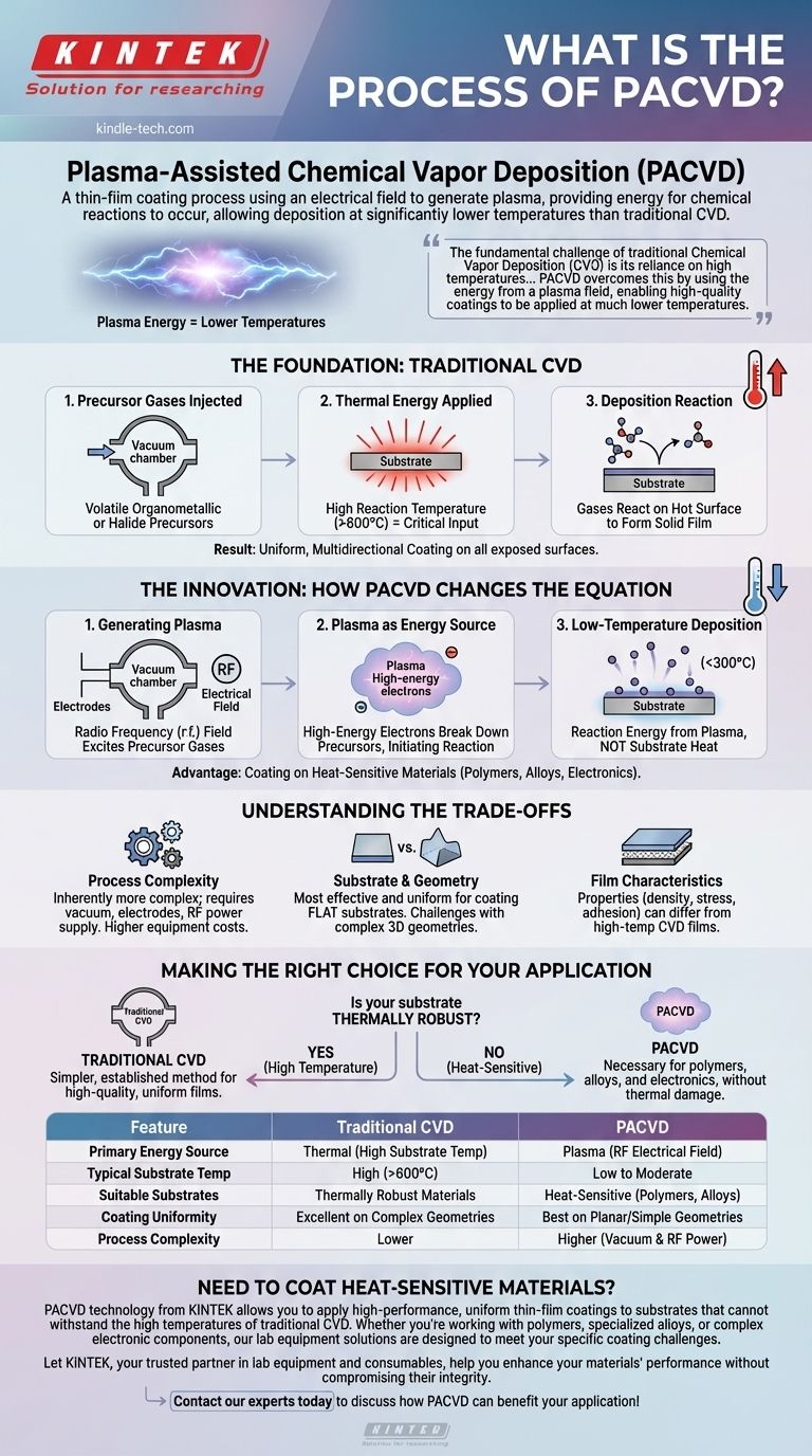
Plasma-Assisted Chemical Vapor Deposition (PACVD) is a thin-film coating process that uses an electrical field to generate a plasma, which provides the energy for chemical reactions to occur. Unlike traditional Chemical Vapor Deposition (CVD) that relies solely on high heat, PACVD allows precursor gases to react and deposit onto a substrate at significantly lower temperatures.
The fundamental challenge of traditional Chemical Vapor Deposition (CVD) is its reliance on high temperatures, which can damage sensitive materials. PACVD overcomes this by using the energy from a plasma field, enabling high-quality coatings to be applied at much lower temperatures.
The Foundation: Understanding Traditional CVD
To grasp the innovation of PACVD, one must first understand the principles of conventional Chemical Vapor Deposition (CVD). It is a widely used industrial process for creating high-performance solid films.
Introducing Precursor Gases
The process begins by injecting volatile precursor gases into a reaction chamber under vacuum. These precursors are typically organometallic or halide compounds that contain the elements of the desired coating.
The Role of Thermal Energy
In traditional CVD, one or more substrates within the chamber are heated to a high reaction temperature. This thermal energy is the critical input that drives the entire process.
The Deposition Reaction
The intense heat causes the precursor gases to react or decompose directly on the hot substrate's surface. This chemical reaction results in the formation of a solid material that bonds to the surface.
A Uniform, Multidirectional Coating
Over time, this process builds up a thin, uniform, and high-purity film. Because the deposition is driven by a chemical reaction in a vapor phase, the coating forms evenly on all exposed surfaces of the component, distinguishing it from line-of-sight methods.
The Innovation: How PACVD Changes the Equation
PACVD is a direct evolution of CVD, designed specifically to eliminate the need for extremely high substrate temperatures. It achieves this by introducing a new form of energy into the system.
Generating the Plasma
A PACVD system operates in a vacuum chamber containing two electrodes. A radio frequency (r.f.) electrical field is applied to these electrodes, which excites the precursor gases into a plasma state.
Plasma as the Energy Source
This plasma is a partially ionized gas containing high-energy electrons. These electrons, not thermal energy from the substrate, provide the necessary energy to break down the precursor gas molecules and initiate the chemical reaction.
The Low-Temperature Advantage
Because the reaction energy comes from the plasma itself, the substrate can remain at a much lower temperature. This allows for the deposition of high-quality thin films on materials that would otherwise melt, warp, or be damaged by the heat of traditional CVD.
Understanding the Trade-offs
While the low-temperature capability of PACVD is a significant advantage, it's important to understand the associated considerations.
Process Complexity
A PACVD system is inherently more complex than a standard thermal CVD furnace. It requires a vacuum chamber, electrodes, and a radio frequency power supply, which can increase equipment and operational costs.
Substrate and Geometry
The plasma field is most effective and uniform between planar electrodes. This makes the process exceptionally well-suited for coating flat substrates but can present challenges for highly complex, three-dimensional geometries.
Film Characteristics
The properties of a film deposited via PACVD—such as density, internal stress, and adhesion—can differ from a film created by high-temperature CVD. These differences must be accounted for depending on the specific performance requirements of the final product.
Making the Right Choice for Your Application
Choosing between traditional CVD and PACVD hinges on a single, critical factor: the thermal stability of your substrate.
- If your substrate is thermally robust and can withstand high temperatures: Traditional CVD is often a simpler and more established method for achieving high-quality, uniform films.
- If your substrate is heat-sensitive (like polymers, certain alloys, or complex electronics): PACVD is the necessary choice, as it provides the reaction energy without requiring damaging high temperatures.
Ultimately, your decision is dictated by the thermal limitations of your substrate, with PACVD providing a critical solution for temperature-sensitive applications.
Summary Table:
| Feature | Traditional CVD | PACVD |
|---|---|---|
| Primary Energy Source | Thermal (High Substrate Temperature) | Plasma (RF Electrical Field) |
| Typical Substrate Temperature | High (Often > 600°C) | Low to Moderate |
| Suitable Substrates | Thermally Robust Materials | Heat-Sensitive Materials (Polymers, Certain Alloys) |
| Coating Uniformity | Excellent on Complex Geometries | Best on Planar or Simple Geometries |
| Process Complexity | Lower | Higher (Requires Vacuum & RF Power Supply) |
Need to Coat Heat-Sensitive Materials?
PACVD technology from KINTEK allows you to apply high-performance, uniform thin-film coatings to substrates that cannot withstand the high temperatures of traditional CVD. Whether you're working with polymers, specialized alloys, or complex electronic components, our lab equipment solutions are designed to meet your specific coating challenges.
Let KINTEK, your trusted partner in lab equipment and consumables, help you enhance your materials' performance without compromising their integrity.
Contact our experts today to discuss how PACVD can benefit your application!
Visual Guide
Related Products
- Inclined Rotary Plasma Enhanced Chemical Vapor Deposition PECVD Equipment Tube Furnace Machine
- Inclined Rotary Plasma Enhanced Chemical Vapor Deposition PECVD Equipment Tube Furnace Machine
- RF PECVD System Radio Frequency Plasma-Enhanced Chemical Vapor Deposition RF PECVD
- Chemical Vapor Deposition CVD Equipment System Chamber Slide PECVD Tube Furnace with Liquid Gasifier PECVD Machine
- Microwave Plasma Chemical Vapor Deposition MPCVD Machine System Reactor for Lab and Diamond Growth
People Also Ask
- How does plasma vapor deposition work? A Low-Temperature Coating Solution for Sensitive Materials
- How does the PECVD function enhance thin-film properties? Achieve Superior Chemical Stability & Durability
- How does plasma enhance CVD? Unlock Low-Temperature, High-Quality Film Deposition
- What is plasma enhanced chemical vapor deposition PECVD equipment? A Guide to Low-Temperature Thin Film Deposition
- What is plasma activated chemical vapour deposition method? A Low-Temperature Solution for Advanced Coatings


