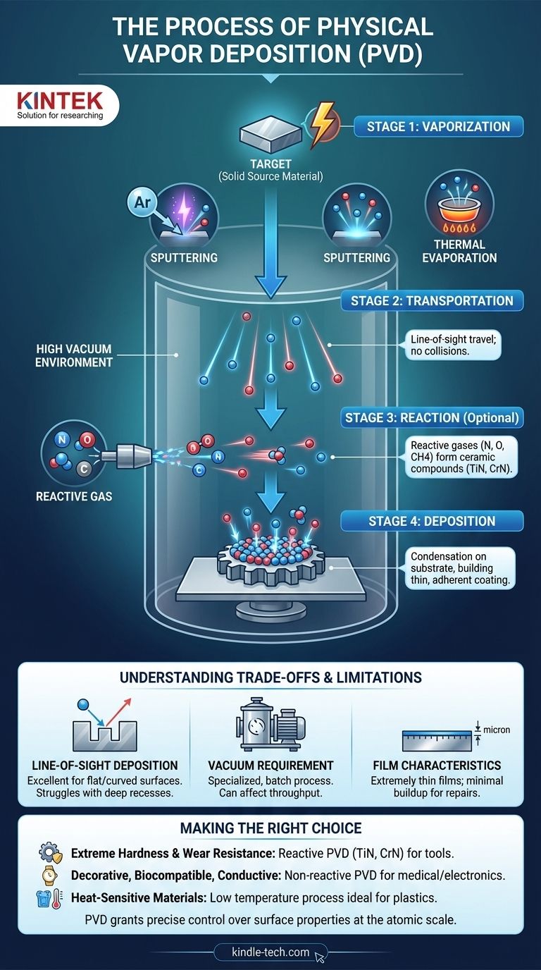
In essence, the Physical Vapor Deposition (PVD) process is a vacuum-based technique for applying an exceptionally thin, high-performance coating to a surface. The core of the process involves four stages: turning a solid source material into a vapor (Vaporization), moving that vapor to the part being coated (Transportation), sometimes reacting it with a gas to form a new compound (Reaction), and finally condensing the vapor onto the part's surface, building the coating atom by atom (Deposition).
PVD is best understood not as a simple coating method, but as an atomic-level construction process. It takes place in a high vacuum, allowing individual atoms from a source material to travel in a straight line and build up on a substrate, forming a dense, pure, and highly adherent film.
The Four Core Stages of PVD
The PVD process can be broken down into a sequence of four distinct, highly controlled stages. Each stage is critical to achieving the final properties of the coating.
Stage 1: Vaporization - Creating the Building Blocks
The process begins by converting a solid source material, known as the target, into a gaseous vapor. This is not like boiling water; it's a high-energy physical process.
This is typically achieved through one of two primary methods:
- Sputtering: An energized, inert gas (like Argon) is introduced into the vacuum chamber, creating a plasma. Ions from this plasma are accelerated into the target, striking it with enough force to knock individual atoms loose, like a cue ball breaking a rack of billiard balls.
- Thermal Evaporation: The target material is heated in the vacuum using methods like resistive heating or an electron beam until it "boils" and releases atoms as a vapor.
Stage 2: Transportation - The Journey Through a Vacuum
Once the atoms are freed from the target, they travel through the vacuum chamber toward the substrate (the part being coated).
The high-vacuum environment is non-negotiable. It ensures there are no air molecules for the vaporized atoms to collide with, allowing them to travel in a straight, unimpeded "line-of-sight" path from the target to the substrate.
Stage 3: Reaction - Customizing the Coating Chemistry
This stage is what defines Reactive PVD and is key to creating many of the hardest and most durable coatings. It is an optional but powerful step.
During transport, a reactive gas (like nitrogen, oxygen, or methane) can be precisely introduced into the chamber. The vaporized metal atoms react with this gas mid-flight or on the substrate surface to form a new ceramic compound. For example, titanium vapor reacting with nitrogen gas forms the gold-colored, ultra-hard Titanium Nitride (TiN).
Stage 4: Deposition - Building the Film Atom by Atom
When the vaporized atoms (or newly formed compound molecules) reach the cooler surface of the substrate, they condense back into a solid state.
This condensation builds the coating one atomic layer at a time. The result is an extremely thin, dense, and uniform film that bonds tightly to the substrate's surface. The entire process results in coatings that are often only a few microns thick.
Understanding the Trade-offs and Limitations
While powerful, the PVD process has inherent characteristics that make it suitable for some applications but not others. Understanding these trade-offs is key to making an informed decision.
Line-of-Sight Deposition
Because the coating atoms travel in a straight line, PVD is excellent for coating flat or externally curved surfaces. However, it struggles to coat deep recesses, internal bores, or complex, shadowed geometries. The parts often need to be rotated on complex fixtures to ensure even coverage.
The Vacuum Requirement
Creating and maintaining a high vacuum requires specialized, expensive equipment. This makes PVD a batch process, not a continuous one, which can affect throughput and cost compared to methods like electroplating.
Film Characteristics
PVD films are extremely thin. While this is an advantage for maintaining the dimensional tolerance of precision parts, they offer minimal buildup for repairing damaged or worn surfaces.
Making the Right Choice for Your Application
Selecting the right coating process depends entirely on your end goal. PVD excels where precision, purity, and high performance are paramount.
- If your primary focus is extreme hardness and wear resistance: Reactive PVD is the solution for creating ceramic coatings like Titanium Nitride (TiN) or Chromium Nitride (CrN) on cutting tools and industrial components.
- If your primary focus is a decorative, biocompatible, or conductive layer: Non-reactive PVD is used to deposit pure, thin layers of metals like titanium, gold, or aluminum for medical implants, watches, and electronics.
- If your primary focus is coating heat-sensitive materials: The relatively low temperature of the PVD process makes it ideal for coating plastics or other materials that would be damaged by high-heat processes.
Ultimately, PVD is a sophisticated manufacturing tool that grants precise control over a material's surface properties at the atomic scale.
Summary Table:
| Stage | Key Process | Purpose |
|---|---|---|
| 1. Vaporization | Sputtering or Thermal Evaporation | Convert solid target material into atomic vapor |
| 2. Transportation | High-vacuum line-of-sight travel | Move vapor atoms to substrate without interference |
| 3. Reaction (Optional) | Introduction of reactive gases | Form ceramic compounds like TiN or CrN |
| 4. Deposition | Condensation on substrate surface | Build thin, dense, adherent coating atom by atom |
Ready to enhance your products with high-performance PVD coatings?
At KINTEK, we specialize in precision lab equipment and coating solutions for laboratories and manufacturers. Our expertise in PVD technology can help you achieve superior surface properties for your applications, whether you need extreme wear resistance, decorative finishes, or biocompatible layers.
We provide:
- Advanced PVD systems for research and production
- Expert consultation on coating selection and process optimization
- Solutions for cutting tools, medical devices, electronics, and more
Let's discuss how PVD can solve your specific surface engineering challenges. Contact our experts today for a personalized consultation!
Visual Guide
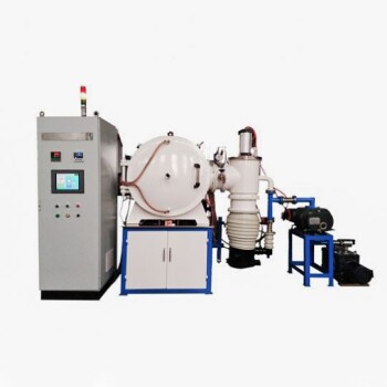
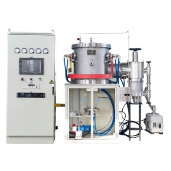
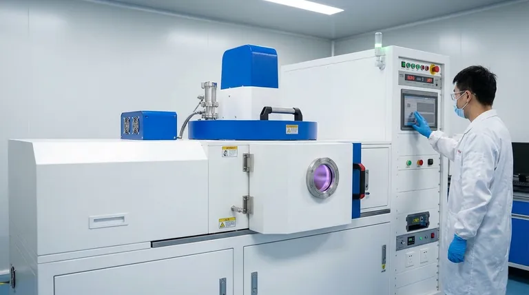
Related Products
- RF PECVD System Radio Frequency Plasma-Enhanced Chemical Vapor Deposition RF PECVD
- Chemical Vapor Deposition CVD Equipment System Chamber Slide PECVD Tube Furnace with Liquid Gasifier PECVD Machine
- Split Chamber CVD Tube Furnace with Vacuum Station Chemical Vapor Deposition System Equipment Machine
- Aluminized Ceramic Evaporation Boat for Thin Film Deposition
- 1400℃ Controlled Atmosphere Furnace with Nitrogen and Inert Atmosphere
People Also Ask
- Why is PECVD environment friendly? Understanding the Eco-Friendly Benefits of Plasma-Enhanced Coating
- How does RF power create plasma? Achieve Stable, High-Density Plasma for Your Applications
- What are the benefits of PECVD? Achieve Superior Low-Temperature Thin Film Deposition
- How are PECVD and CVD different? A Guide to Choosing the Right Thin-Film Deposition Process
- What are the applications of PECVD? Essential for Semiconductors, MEMS, and Solar Cells