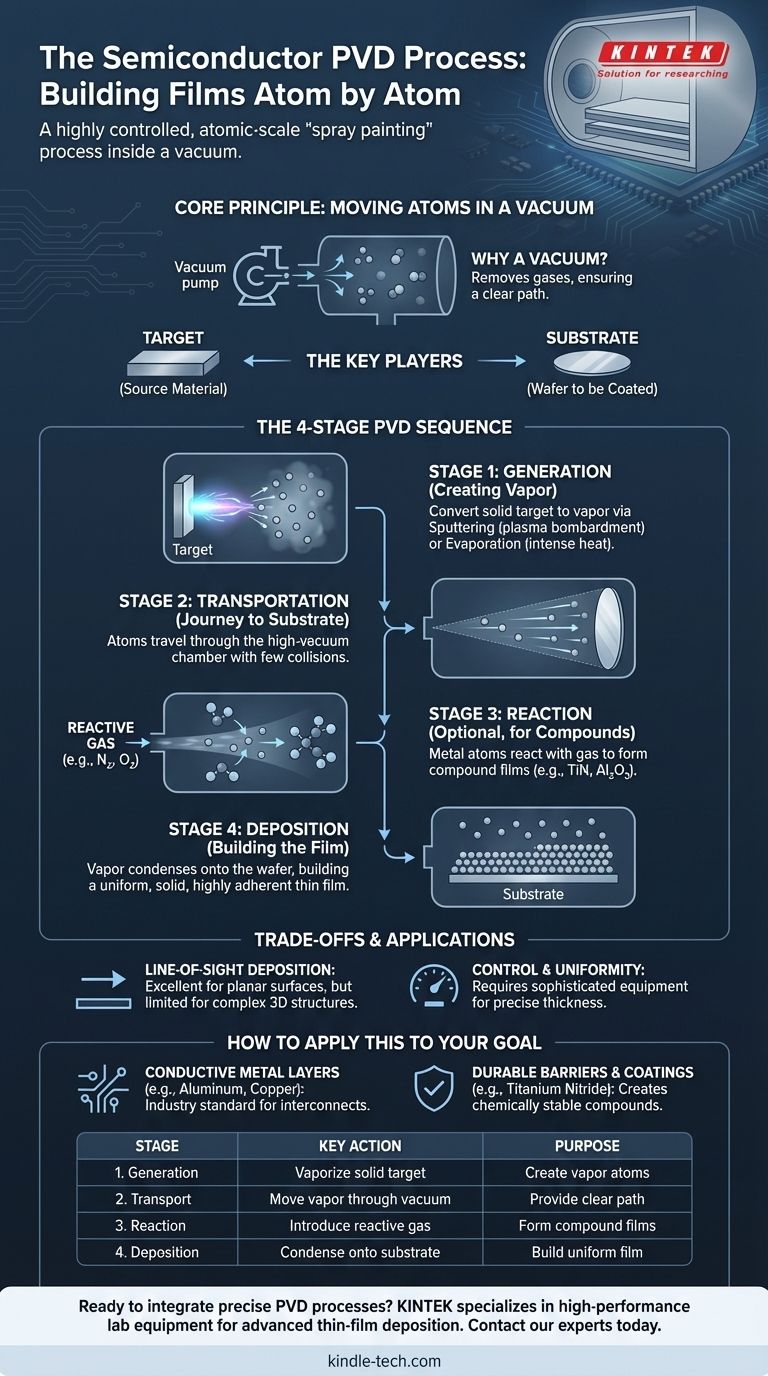
At its core, the Physical Vapor Deposition (PVD) process in semiconductor manufacturing is a vacuum deposition technique that builds an ultra-thin film on a substrate, or wafer, one atom at a time. The process consists of four fundamental stages: generating a vapor from a solid source material, transporting that vapor through a vacuum, allowing it to react with gases if necessary, and finally, depositing it as a solid film onto the substrate's surface.
PVD is best understood as a highly controlled, atomic-scale "spray painting" process inside a vacuum. It physically moves material from a source (the "target") to a destination (the "substrate") without fundamental chemical reactions, resulting in an exceptionally pure and uniform thin film.
The Core Principle: Moving Atoms in a Vacuum
Before breaking down the steps, it's critical to understand the environment in which PVD occurs. The entire process is fundamentally dependent on the physics of a high-vacuum chamber.
Why a Vacuum is Non-Negotiable
A vacuum, or very low-pressure environment, is essential because it removes air and other gas molecules. This creates a clear, unobstructed path for the vaporized atoms to travel from their source to the target wafer.
Without a vacuum, the vaporized atoms would collide with billions of air particles, scattering them and preventing the formation of a uniform, dense film.
The Key Players: Target and Substrate
The process involves two primary components:
- The Target: This is a piece of the pure, solid source material you want to deposit (e.g., aluminum, titanium, copper).
- The Substrate: This is the object being coated, which in semiconductor fabrication is the silicon wafer.
Deconstructing the Four Stages of PVD
While the concept is straightforward, the execution is a precise, four-stage sequence.
Stage 1: Generation (Creating the Vapor)
The first step is to convert the solid target material into a vapor. This is accomplished by bombarding the target with a high-energy source.
The two most common generation methods in semiconductor PVD are sputtering and evaporation. Sputtering uses energized plasma to physically knock atoms off the target's surface, much like a microscopic sandblaster. Evaporation uses intense heat to effectively boil the material, releasing atoms as a gas.
Stage 2: Transportation (The Journey to the Substrate)
Once liberated from the target, the vaporized atoms or molecules travel through the vacuum chamber.
Because of the high vacuum, these particles move in a straight line with few or no collisions until they reach the substrate.
Stage 3: Reaction (An Optional but Critical Step)
This stage is what defines different types of PVD. For depositing a pure metal film like aluminum, this step does not occur.
However, if the goal is to create a compound film, a reactive gas (like nitrogen or oxygen) is introduced into the chamber. The metal atoms react with this gas during transport to form materials like titanium nitride (TiN) or aluminum oxide (Al₂O₃).
Stage 4: Deposition (Building the Film)
In the final stage, the vapor stream reaches the cooler substrate and condenses, changing back into a solid state.
This condensation builds up layer by layer, atom by atom, to form a thin, solid, and highly adherent film on the wafer's surface.
Understanding the Trade-offs and Limitations
While powerful, PVD is not without its challenges. Understanding its limitations is key to its proper application.
Line-of-Sight Deposition
Because the vapor travels in a straight line, PVD is a line-of-sight technique. This means it excels at coating flat, planar surfaces.
However, it struggles to uniformly coat complex 3D structures with deep trenches or overhangs. Areas not in the direct path of the vapor stream receive little to no coating, an issue known as the "shadowing effect."
Control and Uniformity
Achieving perfect film thickness and uniformity across an entire large-diameter wafer (e.g., 300mm) requires highly sophisticated equipment and process control. Minor variations in temperature, pressure, or plasma density can affect the final result.
How to Apply This to Your Goal
PVD is a foundational tool in microfabrication, chosen for specific, well-defined purposes.
- If your primary focus is creating conductive metal layers: PVD is the industry standard for depositing pure metals like aluminum or copper, which form the wiring (interconnects) that connects transistors on a chip.
- If your primary focus is forming a durable barrier or coating: Reactive PVD is used to create hard, chemically stable compounds like Titanium Nitride (TiN), which acts as a diffusion barrier to prevent different materials from mixing.
Ultimately, PVD is the definitive physical method for building the ultra-thin, high-purity films that are the building blocks of modern electronic devices.
Summary Table:
| Stage | Key Action | Purpose |
|---|---|---|
| 1. Generation | Vaporize solid target material | Create a vapor of source atoms |
| 2. Transport | Move vapor through a vacuum | Provide a clear path to the substrate |
| 3. Reaction | Introduce reactive gas (if needed) | Form compound films (e.g., TiN) |
| 4. Deposition | Condense vapor onto substrate | Build a uniform, solid thin film |
Ready to integrate precise PVD processes into your semiconductor fabrication? KINTEK specializes in high-performance lab equipment and consumables for advanced thin-film deposition. Our solutions ensure the purity and uniformity critical for your semiconductor R&D and production. Contact our experts today to discuss how we can support your laboratory's specific PVD requirements.
Visual Guide
Related Products
- 915MHz MPCVD Diamond Machine Microwave Plasma Chemical Vapor Deposition System Reactor
- HFCVD Machine System Equipment for Drawing Die Nano-Diamond Coating
- Vacuum Hot Press Furnace Machine for Lamination and Heating
- Custom PTFE Wafer Holders for Lab and Semiconductor Processing
- Benchtop Laboratory Vacuum Freeze Dryer
People Also Ask
- How does chemical vapor deposition work for diamonds? Grow Lab-Created Diamonds Layer by Layer
- How difficult is it to grow a diamond? The Immense Challenge of Atomic-Level Precision
- What is MPCVD method? A Guide to High-Purity Diamond Synthesis
- What are the limitations of diamonds? Beyond the Myth of Perfection
- How does MPCVD work? A Guide to Low-Temperature, High-Quality Film Deposition