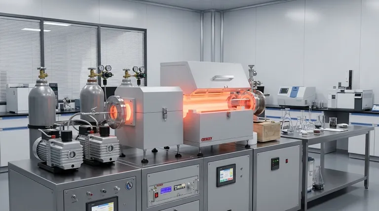
At its core, silicon deposition is the process of applying a thin, uniform layer of silicon onto a surface, known as a substrate. This foundational technique in modern manufacturing follows a sequence of highly controlled steps: preparing a pure silicon source and a clean substrate, transporting silicon atoms or molecules to the substrate within a controlled environment, and building the film layer by layer.
The specific deposition method you choose is not arbitrary; it is dictated by the final properties the silicon film must have. The fundamental choice between physical and chemical deposition techniques determines the film's purity, crystal structure, and suitability for its end use, from microchips to solar panels.
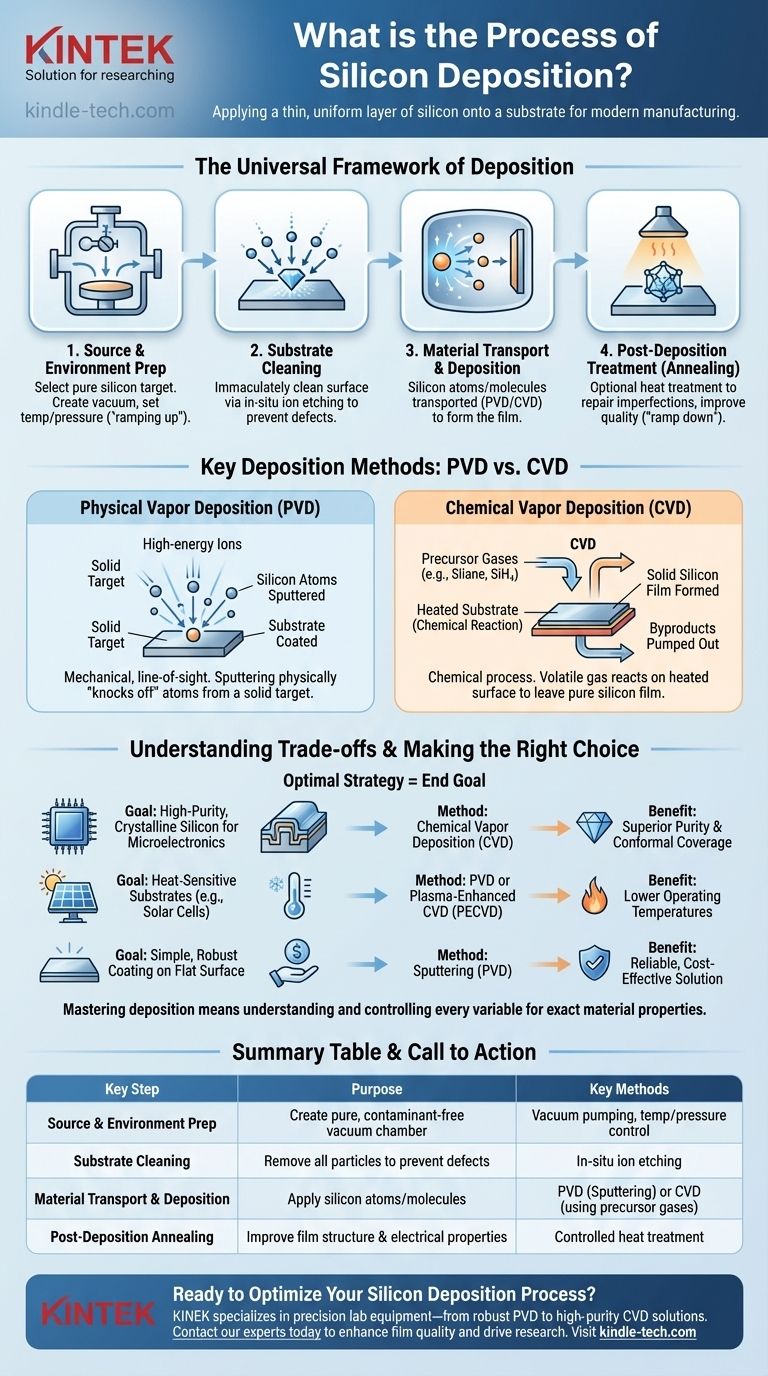
The Universal Framework of Deposition
While specific techniques vary, nearly all silicon deposition processes follow a universal, multi-stage framework. Each step is critical for achieving the desired film quality and performance characteristics.
Step 1: Source Material & Environment Preparation
The process begins by selecting a high-purity silicon source, often called a "target." Simultaneously, the deposition chamber is prepared. This typically involves creating a vacuum to remove contaminants and setting a precise temperature and pressure, a stage known as "ramping up."
Step 2: Substrate Cleaning
Before deposition can begin, the substrate surface must be immaculately clean. Even microscopic particles or residue will cause defects in the final silicon film. This is often achieved through an in-situ "etching" process, which uses ions to bombard and scrub the substrate surface clean inside the vacuum chamber.
Step 3: Material Transport and Deposition
This is the heart of the process. The silicon source material is energized and transported to the substrate. The method of transport is the primary differentiator between techniques, such as physically knocking atoms off a target (PVD) or using a chemical reaction from a precursor gas (CVD). These atoms or molecules then land on the substrate and form a solid, thin film.
Step 4: Post-Deposition Treatment (Annealing)
After the film is deposited, it may undergo an optional heat treatment called annealing. This step helps repair any structural imperfections and can improve the film's crystalline quality and electrical properties. Finally, the chamber is returned to room temperature and ambient pressure in a controlled "ramp down" phase.
Key Deposition Methods: PVD vs. CVD
The way silicon is transported to the substrate falls into two major categories: Physical Vapor Deposition (PVD) and Chemical Vapor Deposition (CVD). The choice between them is a critical engineering decision.
Physical Vapor Deposition (PVD)
PVD is a mechanical-line-of-sight process. In sputtering, a common PVD method, a solid silicon target is bombarded with high-energy ions. This collision physically "knocks off" or "sputters" silicon atoms, which then travel through the vacuum and coat the substrate.
Chemical Vapor Deposition (CVD)
CVD is a chemical process. In this method, one or more volatile precursor gases (such as silane, SiH₄) are introduced into the chamber. These gases decompose and react on the heated substrate surface, leaving behind a solid film of pure silicon. The other byproducts of the reaction are then pumped out.
Understanding the Trade-offs
Neither PVD nor CVD is universally superior; the right choice depends on the application's specific requirements.
Purity and Conformal Coverage
CVD generally produces films of higher purity and offers superior conformal coverage. This means it can evenly coat complex, three-dimensional surfaces, which is critical for modern microelectronics. PVD is more of a line-of-sight process and struggles to evenly coat shadowed areas of an intricate surface.
Deposition Temperature
Traditional CVD processes require very high substrate temperatures to drive the necessary chemical reactions. This can damage heat-sensitive components or substrates. Many PVD techniques, along with a variant called Plasma-Enhanced CVD (PECVD), can operate at much lower temperatures.
Deposition Rate and Cost
PVD can often achieve higher deposition rates for certain materials, but the equipment can be complex. CVD processes are the workhorse of the semiconductor industry for high-quality silicon, but managing the precursor gases and high temperatures adds to the complexity and cost.
Making the Right Choice for Your Goal
The optimal silicon deposition strategy is determined entirely by your end goal.
- If your primary focus is high-purity, crystalline silicon for microelectronics: Chemical Vapor Deposition (CVD) is the industry standard for its exceptional purity and ability to coat complex structures.
- If your primary focus is depositing on heat-sensitive substrates or for applications like solar cells: Physical Vapor Deposition (PVD) or Plasma-Enhanced CVD (PECVD) are superior choices due to their lower operating temperatures.
- If your primary focus is a simple, robust coating on a flat surface: Sputtering (a PVD method) provides a reliable and often cost-effective solution.
Ultimately, mastering silicon deposition means understanding and precisely controlling every variable in the process to build the exact material properties your technology requires.
Summary Table:
| Key Step | Purpose | Key Methods |
|---|---|---|
| Source & Environment Prep | Create a pure, contaminant-free vacuum chamber | Vacuum pumping, temperature/pressure control |
| Substrate Cleaning | Remove all particles to prevent film defects | In-situ ion etching |
| Material Transport & Deposition | Apply silicon atoms/molecules to the substrate | PVD (Sputtering) or CVD (using precursor gases) |
| Post-Deposition Annealing | Improve film structure and electrical properties | Controlled heat treatment |
Ready to Optimize Your Silicon Deposition Process?
Whether you're developing advanced microelectronics, high-efficiency solar cells, or specialized coatings, choosing the right deposition equipment is critical. KINTEK specializes in precision lab equipment and consumables for all your silicon deposition needs—from robust PVD sputtering systems to high-purity CVD solutions.
Contact our experts today to discuss how our tailored solutions can enhance your film quality, improve throughput, and drive your research or production forward.
Visual Guide
Related Products
- Silicon Carbide (SIC) Ceramic Sheet Wear-Resistant Engineering Advanced Fine Ceramics
- Precision Machined Silicon Nitride (SiN) Ceramic Sheet for Engineering Advanced Fine Ceramics
- Silicon Carbide (SIC) Ceramic Plate for Engineering Advanced Fine Ceramics
- 915MHz MPCVD Diamond Machine Microwave Plasma Chemical Vapor Deposition System Reactor
- Custom CVD Diamond Coating for Lab Applications
People Also Ask
- Why is silicon carbide more efficient? Unlock Higher Power Density with SiC's Superior Material Properties
- What are the applications of silicon carbide? From Abrasives to High-Tech Semiconductors
- What is the process of making silicon carbide? From Raw Materials to Advanced Ceramics
- What are the common uses of silicon carbide? Unlock Extreme Performance in Harsh Environments
- What are the uses of silicon carbide ceramics in different industries? Master Extreme Performance in Aerospace, Semiconductors & More


