At its core, thin film deposition is a family of manufacturing processes used to apply an exceptionally thin layer of material onto a surface, known as a substrate. These layers, ranging from a few atoms to several micrometers thick, are fundamental to creating modern high-technology products, from computer chips to solar panels. The process allows for the precise engineering of a material's properties—such as its electrical conductivity, hardness, or optical behavior—at the nanoscale.
The central challenge of thin film deposition is not simply applying a layer, but choosing the correct method for the job. The vast array of techniques fall into two primary categories—Physical and Chemical Deposition—each with distinct advantages and trade-offs that determine the final quality and performance of the film.
The Two Fundamental Approaches: Physical vs. Chemical
Every deposition technique can be classified by how it transports material to the substrate surface. The distinction between physical and chemical methods is the most important one to understand.
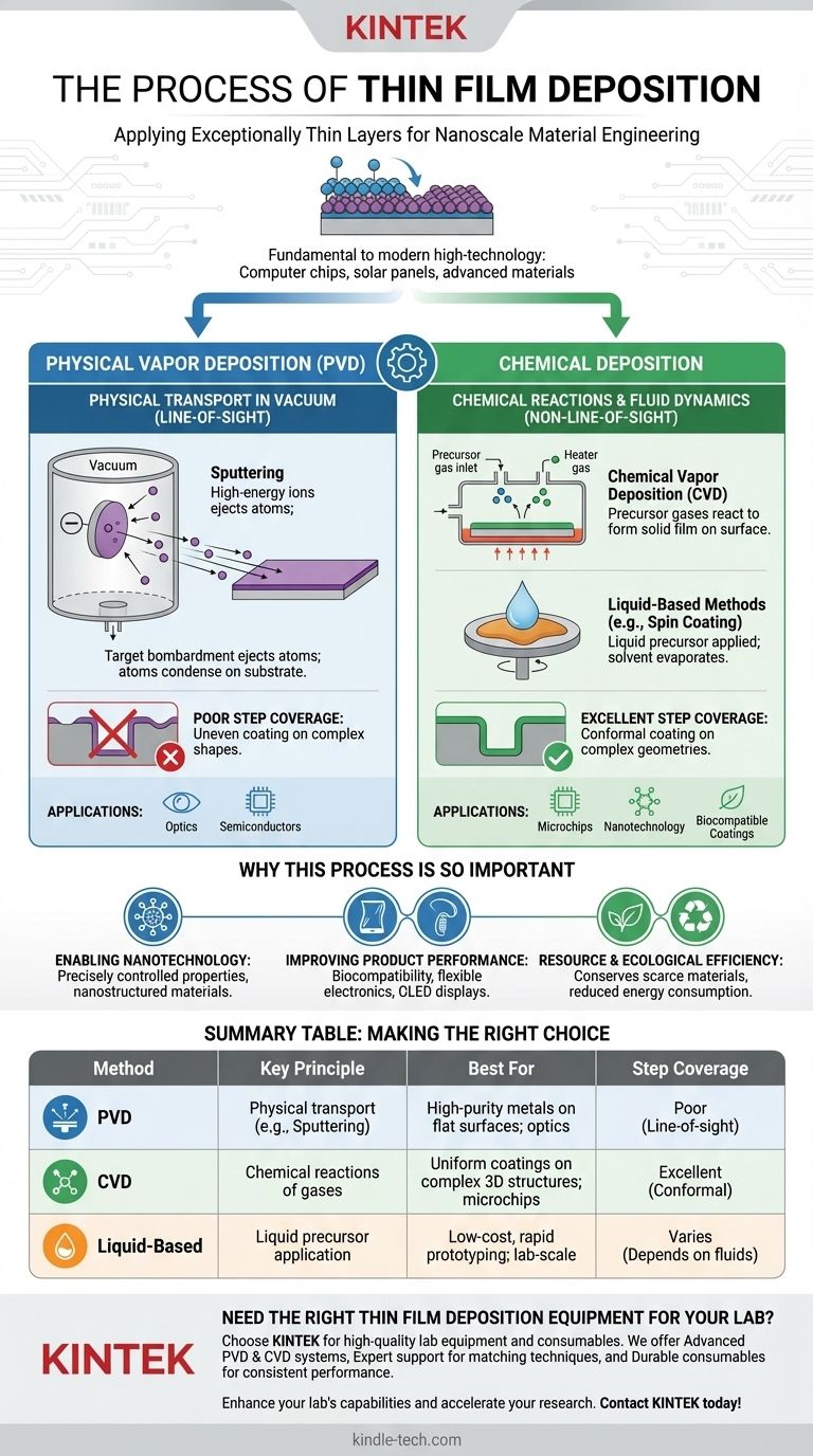
Physical Vapor Deposition (PVD)
PVD techniques involve physically moving atoms or molecules from a source material (the "target") to the substrate, typically within a vacuum. Think of it as a microscopic spray-painting process.
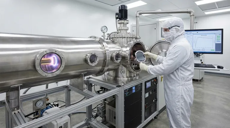
The most common PVD method is sputtering. In this process, the target material is bombarded with high-energy ions, which knock atoms loose. These ejected atoms then travel through the vacuum and condense onto the substrate, forming the thin film.
PVD is often a line-of-sight process, meaning the depositing material travels in a straight line. This can create challenges when coating complex, three-dimensional shapes.
Chemical Deposition
Chemical Deposition techniques use chemical reactions to form the film directly on the substrate's surface. Instead of physically transporting solid material, these methods introduce precursor gases or liquids that react and produce the desired solid film.
A prominent example is Chemical Vapor Deposition (CVD), where gases react in a chamber, and one of the solid byproducts of that reaction forms the film on the heated substrate.
Other simpler methods, like spin coating or drop casting, involve applying a liquid containing the desired material and then allowing the solvent to evaporate, leaving the thin film behind. Because they rely on chemical reactions or fluid dynamics, these methods are often not limited by line-of-sight.
Why This Process is So Important
Thin film deposition is not just an incremental improvement; it is an enabling technology that has unlocked entirely new fields of science and engineering.
Enabling Nanotechnology and Advanced Materials
Deposition allows for the synthesis of nanostructured coatings and materials with precisely controlled properties. This control at the atomic level is the foundation of nanotechnology, enabling the creation of materials that don't exist in nature.
Improving Product Performance and Functionality
Existing products are dramatically improved with thin films. In medicine, films add biocompatibility to implants to prevent rejection by the body or can be designed for controlled drug delivery. In electronics, they are essential for creating semiconductors, flexible solar cells, and OLED displays.
Resource and Ecological Efficiency
By applying only the material that is needed, thin film deposition is an excellent way to conserve scarce or expensive materials. Many modern processes are also designed to reduce energy consumption and effluent output compared to traditional bulk manufacturing.
Understanding the Trade-offs
Choosing a deposition method involves balancing competing factors. No single technique is perfect for every application, and understanding the trade-offs is critical for success.
The Challenge of Step Coverage
A key metric is step coverage, also known as fill capability. It measures how uniformly a film coats a substrate with uneven topography, like the trenches and vias on a microchip.
It is calculated as the ratio of the film's thickness on the sides or bottom of a feature compared to its thickness on the flat, open top surface. A ratio of 1 indicates perfect, uniform coverage.
PVD vs. Chemical Deposition: A Coverage Comparison
Because PVD methods like sputtering are line-of-sight, they often result in poor step coverage. The top surfaces receive the most material, while sidewalls and deep trenches receive very little, creating a thin, weak point in the film.
Chemical methods, especially CVD, are generally superior for complex surfaces. The precursor gases can flow into and react within intricate geometries, resulting in a much more uniform and conformal coating.
Other Factors: Cost, Purity, and Rate
The choice also depends on other factors. PVD can produce films of extremely high purity, which is critical for many optical and electronic applications. However, chemical methods can sometimes offer higher deposition rates and lower equipment costs, making them more suitable for large-scale production.
Making the Right Choice for Your Goal
Your application's specific requirements will dictate the best deposition strategy.
- If your primary focus is coating complex 3D structures uniformly: A chemical method like CVD is often the superior choice due to its non-line-of-sight, conformal nature.
- If your primary focus is depositing a high-purity metal or alloy onto a relatively flat surface: A physical method like sputtering provides excellent control and is an industry standard for optics and semiconductors.
- If your primary focus is low-cost, rapid prototyping in a lab setting: Simple liquid-based techniques like spin coating or drop casting can provide a functional film without the need for complex vacuum equipment.
Ultimately, mastering thin film deposition means matching the right technique to the specific engineering challenge at hand.
Summary Table:
| Deposition Method | Key Principle | Best For | Step Coverage |
|---|---|---|---|
| Physical Vapor Deposition (PVD) | Physically transports atoms from a target to substrate in a vacuum (e.g., sputtering). | High-purity metals on flat surfaces; optics, semiconductors. | Poor (line-of-sight) |
| Chemical Vapor Deposition (CVD) | Uses chemical reactions of gases to form a film on the substrate. | Uniform coatings on complex 3D structures; microchips, nanotechnology. | Excellent (conformal) |
| Liquid-Based Methods (e.g., Spin Coating) | Applies a liquid precursor; solvent evaporates to leave a thin film. | Low-cost, rapid prototyping; lab-scale applications. | Varies (depends on fluid dynamics) |
Need the Right Thin Film Deposition Equipment for Your Lab?
Choosing the correct deposition method is critical for your project's success, whether you require the high purity of PVD sputtering or the uniform coverage of CVD. KINTEK specializes in providing high-quality lab equipment and consumables tailored to your thin film deposition needs.
We help laboratories achieve precise, reliable results with:
- Advanced PVD and CVD systems for research and production.
- Expert support to match the best technique to your application—from semiconductors to biocompatible coatings.
- Durable consumables and targets to ensure consistent performance.
Enhance your lab's capabilities and accelerate your research. Contact KINTEK today to discuss your specific requirements and discover how our solutions can drive your innovations forward!
Visual Guide
Related Products
- Aluminized Ceramic Evaporation Boat for Thin Film Deposition
- Tungsten Evaporation Boat for Thin Film Deposition
- Electron Beam Evaporation Coating Oxygen-Free Copper Crucible and Evaporation Boat
- Molybdenum Tungsten Tantalum Evaporation Boat for High Temperature Applications
- Vacuum Hot Press Furnace Machine for Lamination and Heating
People Also Ask
- Why is an alumina boat and Ti3AlC2 powder bed necessary for Ti2AlC sintering? Protect MAX Phase Purity
- What is the widely used boat made of in thermal evaporation? Choosing the Right Material for High-Purity Deposition
- What is the chemical method for thin film deposition? Build Films from the Molecular Level Up
- What are the alternatives to sputtering? Choose the Right Thin Film Deposition Method
- Why are high-purity ceramic boats used for lignin activation? Ensure Purity & Thermal Stability


