The formation of a thin film is a multi-stage process where a source material is transported through a controlled medium, such as a vacuum, and deposited atom by atom onto a prepared surface, known as a substrate. This process can be followed by heat treatments to refine the film's properties, which are then analyzed to ensure they meet specific functional requirements.
Thin film formation is not merely a coating technique; it is the atomic-level engineering of a material's surface. The fundamental choice between physical or chemical deposition methods is the most critical decision, as it directly dictates the film's final structure, quality, and performance.
The Foundational Stages of Film Creation
The creation of any thin film, regardless of the specific technique, follows a logical progression from raw material to a functional, engineered surface. Each stage presents critical variables that influence the final outcome.
Step 1: Source Material and Substrate Preparation
The process begins by selecting a pure source material, often called a target, which can be a metal or a dielectric compound. The choice of material is entirely dependent on the desired function of the final film.
Simultaneously, the substrate—the base material onto which the film is grown—must be meticulously cleaned and prepared to ensure proper adhesion and uniform film growth.
Step 2: Transport and Deposition
The core of the process involves liberating atoms or molecules from the source material and transporting them to the substrate. This almost always occurs within a highly controlled environment, typically a vacuum chamber, to prevent contamination.
The method of transport and deposition is the primary differentiator between the various thin film technologies.
Step 3: Post-Deposition Treatment
Once the film has been deposited to the desired thickness, it may undergo optional treatments to refine its properties. Annealing, a form of heat treatment, can help improve the film's crystalline structure and reduce internal stress.
The Two Primary Deposition Paradigms
While there are many specific techniques, they almost all fall into two major categories: physically dislodging atoms from a source or using a chemical reaction to build the film.
Physical Vapor Deposition (PVD)
PVD methods use mechanical, thermal, or electrostatic means to transfer material. The most common technique is sputtering.
In sputtering, high-energy ions are accelerated towards the source target. The impact physically knocks atoms off the target's surface, which then travel through the vacuum and deposit onto the substrate, building the film layer by layer.
Chemical Vapor Deposition (CVD)
CVD builds a film through a chemical reaction at the substrate's surface. Precursor gases are introduced into a reactor chamber, where they decompose and react on the heated substrate.
For example, to create a silicon film, silane gas (SiH4) is used. For more complex crystalline semiconductors like gallium arsenide, Metalorganic CVD (MOCVD) is employed, which allows for precise, layered growth.
Key Factors That Define Film Quality
The final characteristics of a thin film are not intrinsic to the material alone. They are a product of the entire deposition environment and process.
The Substrate Foundation
The underlying properties of the substrate material, its crystal structure, and its surface smoothness have a profound impact on how the film grows and adheres. The film often inherits characteristics from its foundation.
Deposition Technique and Parameters
The choice between PVD and CVD is fundamental. Beyond that, parameters like vacuum pressure, temperature, gas flow rates, and deposition speed must be precisely controlled by sophisticated equipment to achieve repeatable results.
Film Thickness
The thickness of the film is a critical design parameter. It directly influences the film's optical, electrical, and mechanical properties, causing significant variations in performance even with the same material.
Understanding the Trade-offs and Challenges
Creating a perfect thin film requires navigating a series of technical compromises and potential pitfalls. Each approach has inherent strengths and weaknesses.
PVD: Line-of-Sight Limitations
Sputtering and other PVD techniques are generally "line-of-sight" processes. The source material travels in a straight line to the substrate, which can make it difficult to uniformly coat complex, three-dimensional shapes.
CVD: Chemical Purity and Cost
CVD can produce exceptionally pure and uniform films, but it relies on volatile and often expensive precursor chemicals. Maintaining the purity of these gases is critical, as any contamination can be incorporated into the film, degrading its performance.
The Role of Vacuum Integrity
Nearly all high-performance deposition processes occur in a high or ultra-high vacuum. Any leak or outgassing from chamber components can introduce contaminants that ruin the film. The quality of the vacuum system is paramount to the quality of the final product.
Making the Right Choice for Your Application
Your ultimate goal dictates the ideal deposition strategy. The application's requirements—be they optical, electronic, or mechanical—will guide your selection of material and method.
- If your primary focus is creating durable metallic or dielectric coatings: PVD methods like sputtering are often the most direct and robust choice for their strong adhesion and versatility.
- If your primary focus is growing complex, crystalline semiconductor layers: CVD and its variants are essential for achieving the required chemical precision and structural perfection for electronic devices.
- If your primary focus is achieving specific optical properties: Both methods are viable, but the choice will depend on the material's required refractive index and the need for extremely precise thickness control.
Ultimately, mastering thin film formation is about controlling a sophisticated environment to build functional materials one atomic layer at a time.
Summary Table:
| Stage | Key Process | Key Consideration |
|---|---|---|
| 1. Preparation | Selecting target material & cleaning substrate | Material purity and surface adhesion |
| 2. Deposition | Transporting material in a vacuum (PVD/CVD) | Vacuum integrity and deposition parameters |
| 3. Post-Treatment | Annealing to refine film properties | Temperature control and stress reduction |
| 4. Analysis | Verifying film meets functional requirements | Thickness, uniformity, and performance testing |
Ready to Engineer Your Surface with Precision Thin Films?
The right deposition process is critical to your product's performance. KINTEK specializes in providing the lab equipment and consumables needed for reliable PVD and CVD thin film formation. Whether you are developing semiconductors, optical coatings, or durable surfaces, our expertise ensures you have the control and purity required for success.
Contact us today using the form below to discuss your specific application and discover how KINTEK can support your laboratory's thin film needs.
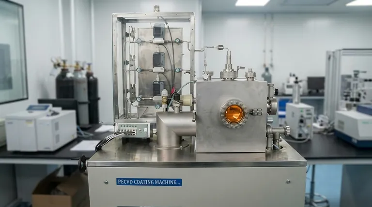
Visual Guide

Related Products
- Aluminized Ceramic Evaporation Boat for Thin Film Deposition
- Tungsten Evaporation Boat for Thin Film Deposition
- Electron Beam Evaporation Coating Oxygen-Free Copper Crucible and Evaporation Boat
- Molybdenum Tungsten Tantalum Evaporation Boat for High Temperature Applications
- Vacuum Hot Press Furnace Machine for Lamination and Heating
People Also Ask
- Why is an alumina boat and Ti3AlC2 powder bed necessary for Ti2AlC sintering? Protect MAX Phase Purity
- What is thin film deposition? Unlock Advanced Surface Engineering for Your Materials
- Why are high-purity ceramic boats used for lignin activation? Ensure Purity & Thermal Stability
- What is the source of evaporation for thin film? Choosing Between Thermal and E-Beam Methods
- What is the chemical method for thin film deposition? Build Films from the Molecular Level Up


